@Daniel Nenni It happened I just found an insightful article you wrote 13 years ago on Semiwiki:
Intel Foundry;
Intel says fabless model collapsing… really? (
Daniel Nenni on 04-28-2012 at 7:00 pm) where there is an interesting discussion in response to the EETimes article: Intel exec says fabless model ‘collapsing’.
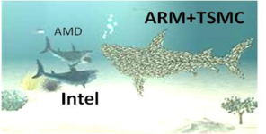
You highlighted with vision, "This is the entire fabless semiconductor ecosystem (Synopsys, Cadence, Mentor, ARM, TSMC, UMC, GlobalFoundries, QCOM, BRCM, NVDA, AMD, and hundreds of other companies) against Intel. Hundreds of billions of dollars in total R&D versus Intel’s billions."
It seems like an unconscious linking of the same thought of yours with another article I posted on LinkedIn: (
Exploring Historical Paradigm Shifts in the Si Foundry Industry.). That article was my private observation and deliberation shared with TSMC’s former Chairman, Dr. Morris Chang, in May 2012:
[My Observation]
How TSMC can in-depth cooperation with eco-customers and eco-partners to jointly define, create and develop performance-differentiated 20nm low-power (e.g. static/standby or dynamic/active power) process flavors are the extremely important strategic challenge for coming years. The future generations of 20nm (i.e. FinFET) shall support to serve optimized low-power consumption (e.g. mobile APU) and high-performance (e.g. NVDA GPGPU) segment technologies ...
Looking back to 2012, surprisedly, TSMC indeed had two major tech nodes at the 20nm Si gate-length process:
• 20nm planar gate, mainly captive run for Apple (a bunt strategy)
• 16nm FinFET (with 20nm gate-length), crowd source serving both low-power consumption (e.g., mobile APU) and high-performance (e.g., NVDA GPGPU) segments with a few different flavors.