Array
(
    [content] => 
    [params] => Array
        (
            [0] => /forum/index.php?threads/which-arrow-lake-and-lunar-lake-chiplets-will-be-fabbed-by-intel.19926/
        )

    [addOns] => Array
        (
            [DL6/MLTP] => 13
            [Hampel/TimeZoneDebug] => 1000070
            [SV/ChangePostDate] => 2010200
            [SemiWiki/Newsletter] => 1000010
            [SemiWiki/WPMenu] => 1000010
            [SemiWiki/XPressExtend] => 1000010
            [ThemeHouse/XLink] => 1000970
            [ThemeHouse/XPress] => 1010570
            [XF] => 2021370
            [XFI] => 1050270
        )

    [wordpress] => /var/www/html
)

Which Arrow Lake and Lunar Lake Chiplets Will be Fabbed by Intel?

fansink

Active member
There are so many conflicting reports, especially since the reports don’t clearly specify Desktop vs Mobile.

It’s reported that the designations may be:

Arrow Lake S - Desktop
Arrow Lake U - Mobile
Lunar Lake ? - Desktop
Lunar Lake MX - Mobile

There are reports that say TSMC will be producing Intel CPUs, GPUs, and NPUs tiles for the Arrow and Lunar Lake platforms.

There are also conflicting reports that Intel will be producing CPU’s for both Arrow and Lunar Lake.

If anyone can answer this, SemiWiki contributors can.

https://www.hardwaretimes.com/intel-15th-gen-core-i9-15900h-24-cores-tsmc-3nm/
https://wccftech.com/intel-ceo-conf...s-next-gen-cpus-n3-arrow-lake-n3b-lunar-lake/
https://wccftech.com/intel-arrow-la...ernative-lunar-lake-intel-3-perf-watt-uplift/
https://www.igorslab.de/en/news-fro...e-cpu-rumors-confirmed-picture-and-schematic/
 
Arrow lake needs to launch (with product available for purchase) in 2H 2024 as committed multiple times by Pat

The links you have are pretty contradictory as are the discussions I have had. The best explanation I have heard is that even Intel employees are not sure of what the SKUs will be. I do know there are multiple mix options for Lunar Lake and Arrow lake. On Meteor Lake the launch plan was changed 5 months before launch. Dont be surprised if you see leaked samples and photos that do not match what is finally launched.
 
1. We’ll know for sure in about 10 months :)

2. It appears to be CPU chiplets only that will be fabbed by Intel directly. But that doesn’t exclude Intel from using TSMC chiplets for some CPU cores as well, Infact depending on volumes it may make the most sense anyway. TSMC N3 appears denser than 20A - good for cost sensitive products, while 20A seems to have higher transistor performance - better for higher end desktop, and possibly higher end mobile.

TSMC has lower power don’t forget. Power seems to be a big concern now that Sam Altman says it is. 😂
 
TSMC 3nm doesn't have backside power delivery, nor does it have GAAFET transistors. Of which Arrow Lake and Lunar Lake are said to have. There would be no reason for the 5 nodes in 4 years if none of those nodes are getting used and it's all being pushed to TSMC. If it's all being pushed to TSMC then Arrow Lake and Lunar Lake do not have the backside power delivery and GAAFET transistors they are meant to have, or TSMC 3nm is suddenly capable of backside power delivery and GAAFET's, both of which is highly doubtful.
 
If Intel was reasonably certain about their 20A/18A prowess, their PR message regarding my question, wouldn't be so ambiguous?
 
If Intel was reasonably certain about their 20A/18A prowess, their PR message regarding my question, wouldn't be so ambiguous?

20A and 18A are totally different animals from a capacity perspective. 20A is a relatively small capacity node (like Intel 4 vs Intel 7); but 18A is planned for (much) higher volume.

The products coming out around ‘the time of 20A’ were also negotiated to be fabbed on TSMC N3 by the prior Intel CEO. The lack of clarity on which products are 20A vs N3 isn’t necessarily a prescription for yields or bullishness, but rather for planned (and previously negotiated) capacity. Intel is likely to have Arrow Lake CPU tiles sourced on 20A and N3, and how many on each is hard to tell since we don’t know 1. Market conditions at year end, 2. What Intel negotiated with TSMC, or 3. What the 20A ramp looks like right now.

Products on 18A are still likely to have specific chiplets/tiles from TSMC, but I think the (Esp. CPU) ratio will shift much more heavily to Intel sourced at that point.

..

FWIW the “leakers” seem fairly bullish on the 20A variant of Arrow Lake vs. Zen 5 on applications, and gaming excepting the X3D variant.
 
Another thing of interest, Intel was meant to benefit from the chiplet design, by reusing SoC and IO tiles from Meteor lake in Arrow Lake, but it turns out those rumours are not true.

When they say “reused”, perhaps Arrow Lake IO is a different physical geometry, since the IO chiplet needs to nest tightly with its new neighbors, yet uses the same architecture or some other features from Meteor Lake, instead of a completely new and improved, thus more costly, IO?
 
When they say “reused”, perhaps Arrow Lake IO is a different physical geometry, since the IO chiplet needs to nest tightly with its new neighbors, yet uses the same architecture or some other features from Meteor Lake, instead of a completely new and improved, thus more costly, IO?
No, they meant actually the same die. You can see here:
"SoC/ IOE 100% reuse from MTL"
 
I find several reasons for grains of salt with these recent leaks, especially comparing Arrow Lake tiles/chipsets to Meteor Lake:

- Why do they need mini dummy dies just to make the final product rectangular under the heat spreader? That's never been required before with multiple die/chiplet setups
- Do we know for sure they're even using Intel packaging and not TSMC for Arrow Lake, given previous deals the previous Intel CEO reached with TSMC?
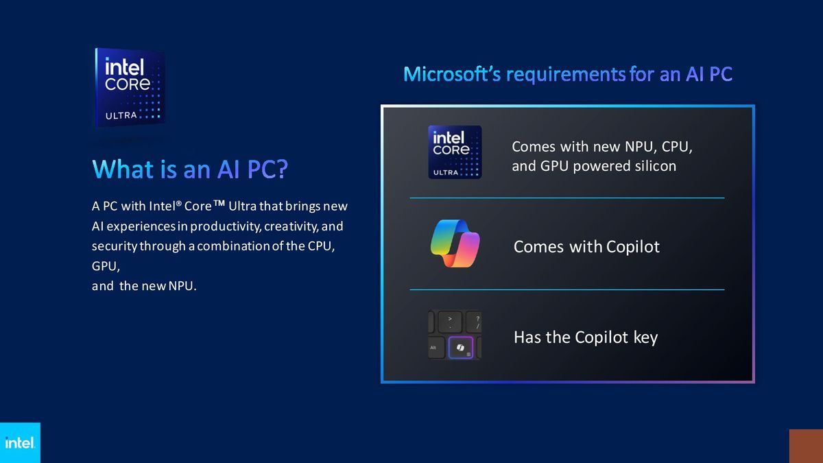
- Lunar Lake is confirmed to have 3x the TOPs of MTL, and presumably Arrow Lake will have an NPU with 3x the TOPS as well to also meet the "next gen PC has 40 TOPs" requirement that Microsoft seems to be outlining. That would mean yet another die change.
- Lunar Lake is going to use Battlemage graphics so the iGPU die will change at least on that product, and possibly for Arrow Lake too

While I think they *could* re-use pieces of the MTL finished product, it doesn't mean they have to (or will)..


"Intel confirms Microsoft's Copilot AI will soon run locally on PCs, next-gen AI PCs require 40 TOPS of NPU performance"

I don't think Intel would want Arrow Lake going out .. not meeting "next gen" specs already
 
Last edited:
Why do they need mini dummy dies just to make the final product rectangular under the heat spreader? That's never been required before with multiple die/chiplet setups
Yes they have. Threadripper had dummy dies, also Meteor lake has one (in some SKUs).
Lunar Lake is confirmed to have 3x the TOPs of MTL, and presumably Arrow Lake will have an NPU with 3x the TOPS as well to also meet the "next gen PC has 40 TOPs" requirement that Microsoft seems to be outlining. That would mean yet another die change.
That's a good point, because the NPU resides in the SoC tile
 
Yes they have. Threadripper had dummy dies, also Meteor lake has one (in some SKUs).

On the flip side, the Ryzen 7000 series dies don't form a rectangle underneath the heatspreadder. Though it does look like Meteor Lake and Lunar Lake both are rectangular.

Those tiny weird dies on Arrow Lake just seem .. fake-ish? Especially the little wedge at the bottom left corner, if that wasn't there, would it really going to prevent the heat spreader from working?

1711885798426.png
 
Especially the little wedge at the bottom left corner, if that wasn't there, would it really going to prevent the heat spreader from working?

Any extra area from the dummies will improve overall heat transfer, by laterally distributing heat, reducing local constriction resistance, especially when exchanging to vapor phase transition (heat pipe) devices.

Compression stress is also improved.
 
Any extra area from the dummies will improve overall heat transfer, by laterally distributing heat, reducing local constriction resistance, especially when exchanging to vapor phase transition (heat pipe) devices.

Compression stress is also improved.

Agreed and makes sense — but is that worth the extra time and cost of adding those extra dummy dies over millions of products? That’s where I’m a little skeptical.

(It may be worth it to Intel - but just thinking that’s extra packaging steps, more time = less volume, more cost).
 
So is the summary that Lunar lake is not Intel Silicon? and that half of Arrow lake will be Intel Silicon?

Dummy are and will continue to be used extensively due to packaging stress and allowing flexibility in SKUs.
 
So is the summary that Lunar lake is not Intel Silicon? and that half of Arrow lake will be Intel Silicon?

Dummy are and will continue to be used extensively due to packaging stress and allowing flexibility in SKUs.

It seems like Intel will be forced to fabricate some Arrow Lake and/or Lunar Lake CPU’s, the easiest being binned low frequency mobile?
 
Supposedly Lunar Lake is just two tiles and the compute tile includes CPU and GPU, that's why they can't use Intel 20A (20A is missing high density libraries needed for the GPU)
 
Intel has advertised both LNL and ARL as 20A which means at least for some models the CPU die will be Intel 20A. Intel has also pre bought a lot of TSMC N3 capacity (and 20A will be ramping) so it looks like some CPU dies for ARL or LNL might also be on TSMC N3.

The other dies are largely looking like TSMC — Battlemage for LNL is TSMC; the NPU die for Meteorlake is based on TSMC so that’ll likely continue (esp with the capacity agreement), etc.

So in terms of total silicon - mostly TSMC; but the CPU dies appear split between Intel and TSMC, but probably favoring Intel.
When did Intel claim LNL is 20A. It showed as external on the roadmaps.

@lefty comments on LNL is aligned with my understanding. It has less chiplets and all are TSMC.

NPU is not a die/Chip. it is a relatively small part of the SOC, correct?

So what fraction of ARL CPUs will be TSMC at launch?
 
When did Intel claim LNL is 20A. It showed as external on the roadmaps.

@lefty comments on LNL is aligned with my understanding. It has less chiplets and all are TSMC.

Apologies - I really had it in my head they showed LNL as 20A but searching around I can’t find proof :(. (I can’t find anything saying it’s exclusively N3 either, but..)
 
Back
Top