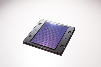
HOKKAIDO, Japan, Dec. 18, 2024 /PRNewswire/ -- Rapidus Corporation, a manufacturer of advanced logic semiconductors, today announced the delivery and installation of ASML's EUV lithography equipment at its Innovative Integration for Manufacturing (IIM-1) foundry, an advanced semiconductor development and manufacturing fab currently under construction in Chitose, Hokkaido. To commemorate the installation, a ceremony was held at Portom Hall in the New Chitose Airport.
This is a significant milestone for Japan's semiconductor industry, marking the first time that an EUV lithography tool will be used for mass production in the country. In addition to the EUV lithography machinery, Rapidus will install additional complementary advanced semiconductor manufacturing equipment, as well as full automated material handling systems in its IIM-1 foundry to optimize 2nm generation gate-all-around (GAA) semiconductor manufacturing.
EUV lithography is one of the key technologies for realizing 2nm semiconductors. An advanced lithography process is critical for forming the 2nm generation GAA structure.
ArF (193nm) immersion exposure has been at the forefront of EUV technology. However, 2nm and future nodes require an even shorter wavelength (13.5nm). The newest generation of EUV lithography technology uses laser sources, optical systems and photomasks that are far more precise than those used previously. The EUV lithography equipment from ASML installed at the Rapidus IIM-1 foundry uses an advanced optical system with a reflective photomask and mirror lenses. It adopts a TWINSCAN platform that performs alignment and scanning on separate stages, realizing increased productivity while responding to shrinking transistor sizes.
A pilot line will begin at Rapidus' IIM-1 in April 2025. A single-wafer process will be introduced for all manufacturing equipment, where Rapidus will proceed with the construction of a new semiconductor foundry service called Rapid and Unified Manufacturing Service (RUMS).
About Rapidus Corporation
Rapidus Corporation aims to develop and manufacture the world's most advanced logic semiconductors. We will create new industries together with our customers through the development and provision of services to shorten cycle times in design, wafer processes, 3D packaging, and more. We will continue to challenge ourselves in order to contribute to the fulfillment, prosperity, and happiness of people's lives through the use of semiconductors.
About Rapidus Corporation
Headquarters:
4-1 Kojimachi, Chiyoda-ku, Tokyo 102-0032, Japan
Establishment:
August 10th, 2022
Executives:
Tetsuro Higashi, Chairman of the Board of Directors
Atsuyoshi Koike, President and Representative Director
]Business:
Research, development, design, manufacture, and sales of semiconductor devices, integrated circuits and other electronic components[/TD]
Capital, etc:
7,346 million yen (as of November 2022)
(includes the amount of capital reserve)
U.S. Media Contact:
Devan Gillick – Breakaway Communications for Rapidus
Email: rapidus@breakawaycom.com
Mobile: (530) 591-3194
SOURCE Rapidus Corporation