You are currently viewing SemiWiki as a guest which gives you limited access to the site. To view blog comments and experience other SemiWiki features you must be a registered member. Registration is fast, simple, and absolutely free so please, join our community today!
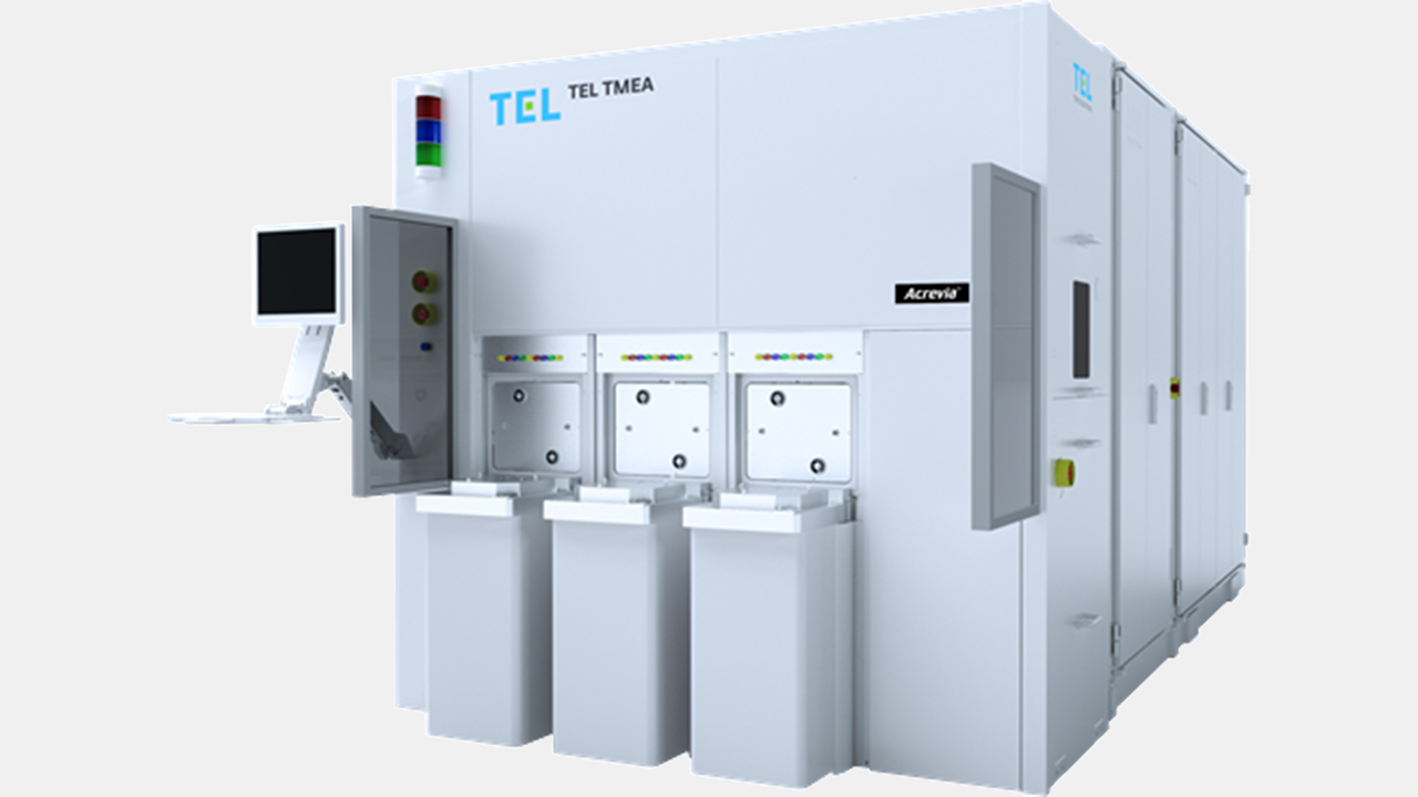
Tokyo Electron Launches Acrevia™, a Gas Cluster Beam System for Ultra-Fine Patterning in EUV Lithography
Tokyo Electron (TEL; Head Office: Minato-ku, Tokyo; President: Toshiki Kawai) today announced the launch of AcreviaTM, a gas cluster beam system designed to modify ultra-fine patterns printed by EUV lithography.
AcreviaTM is a gas cluster beam (GCB) system designed for modifying the critical dimensions and shape of ultra-fine patterns formed by EUV lithography. TEL’s unique GCB technology offers unprecedented low-damage processing and enables further device scaling, yield improvement, and reduced EUV patterning costs for our customers. AcreviaTM is deployed in the semiconductor manufacturing process flow following a single EUV lithography patterning and subsequent dry etching step. The patterned features are irradiated with the directional gas cluster beam, which etches feature sidewalls at an optimal wafer tilting angle to modify critical dimensions and adjust ultra-fine patterns. Acrevia’sTM precise wafer scanning system can control etch amount at any point on the wafer using TEL’s innovative Location Specific Processing (LSP) technology, resulting in unparalleled within wafer uniformity correction capabilities. AcreviaTM can also reduce line edge roughness (LER) on pattern sidewalls, and reduce stochastic litho defects to improve yield.
“Acrevia features our original technology that enables high etch rate and low damage patterning,” says Hiroshi Ishida, General Manager, DSS BU at Tokyo Electron. “In the increasingly challenging field of advanced patterning, Acrevia makes further scaling possible and maximizes productivity. Going forward, we will keep developing technologies that exceed customers’ expectations and contribute to the advancement of semiconductor devices.”
* Gas cluster beam technology: A technology for forming clusters of gas atoms and irradiating them in a high-energy beam for low-damage surface processing
Have to look into more details of the system, but from what TEL posted: "The patterned features are irradiated with the directional gas cluster beam, which etches feature sidewalls at an optimal wafer tilting angle...", sounds similar to AMAT's "pattern shaping" technology.
Have to look into more details of the system, but from what TEL posted: "The patterned features are irradiated with the directional gas cluster beam, which etches feature sidewalls at an optimal wafer tilting angle...", sounds similar to AMAT's "pattern shaping
Have to look into more details of the system, but from what TEL posted: "The patterned features are irradiated with the directional gas cluster beam, which etches feature sidewalls at an optimal wafer tilting angle...", sounds similar to AMAT's "pattern shaping" technology.
I think of it as a nano version of bead blasting to improve the finish of machined parts. It makes the patterns defined by litho and etch smoother. Also can refine/distort the pattern shape (turn circles into ovals). This is a nice description of what a gas cluster beam is https://www.ulvac-phi.com/en/surface-analysis/topics/gcib/