 ASIC or FPGA? Each design style has earned designers’ votes depending on the level of urgency, application complexity and funding of their assigned projects. While it is feasible to transition from ASIC to FPGA design or vice versa, such a move is usually done across project refresh instead of midcourse.
Both Xilinx and Intel(PSG division, formerly from Altera acquisition) are the dominant FPGA vendors representing over 80% of FPGA market share –recently registered $4.52 billion combined annual sales between Q217 until Q118 (which is equivalent to the FPGA market size in 2016 based on Gartner). 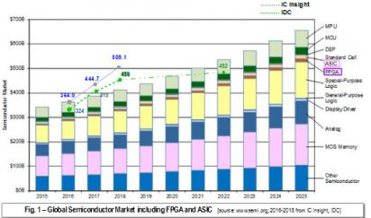 Although it represents only a slice of the global semiconductor market as captured in figure 1, FPGA and ASIC as design implementation vehicles are in high demand and will be around for a while.
As a leading EDA solution provider, Mentor, a Siemens Business commissions Wilson Research Group every two years to conduct a broad, vendor-independent study of design verification practices around the world. Harry Foster, Chief Scientist Verification for the Design Verification Technology Division of Mentor summarized the survey outcomes in this Mentor webinar. In order to provide some contexts on the highlights to be discussed here, let us review the state of our design space.
The computing landscape
There have been plenty narratives asserting the lasting footprints left by our computing technology adoptions. Driven by cost and usage personalization in the mid 80s, our compute system environment shifted from mainframe-centric to workstations. Such migration was then followed by the increased pervasiveness of mobile computing, and the subsequent introduction of cloud computing (which can be perceived as the ‘next-generation mainframe’ with an advanced architecture). Cloud computing allows scalability and provides elastic support to the increasing network of distributed compute clients, accentuated by the proliferation of Internet of Things (IoTs) in the past few years.
Now, with the ever louder drumbeat of AI and data inferencing move to the edge, enabled by the upcoming 5G deployment, once again we slide along this network continuum –to bring about intelligent closer to the data source or else, filter the captured data from dozens of sensors to be more manageable in size and more structured, prior to transporting back to the cloud. It is a data driven computing era with more heterogeneous system, agile data handling, reasonable compute capacity, shorter development cycles and smaller form factor.
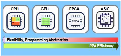
The core enablers As the workhorse of the computing solutions, IC design and its associated implementation methods also align with any paradigm shift on the end-to-end technology use. Since the early days of VLSI design, flexibility provided by Programming Logic Array (PLA) technology and later FPGA (Field Programmable Gate Array) have provided alternatives to full-custom or ASIC design approaches.
During the great push for performance and density aided by Moore’s Law, ASIC design was top on the designers select list. With the recent transition into more data-centric applications, FPGA design adoption has been on the rise –providing solution to data centers as augmented, dedicated accelerators such as for network, search, compute, etc. On the other hand, ASIC designers are faced with shorter development time to develop high-performance and complex designs as the development cost also increases rapidly –making it more prohibitive for cost-sensitive applications.
As FPGA devices have become larger and faster, verifying functionality of costly ASIC designs in FPGAs has become an effective and economical method of verification. However, some ASIC structures cannot be directly implemented in an FPGA efficiently. So the balance of which implementation is more suitable is dependent on the given project criteria: timeline, complexity and budget.
Highlights of the 2018 study
This year 2018 survey outcomes were collected from a total of over 1200 companies globally. More than 45% of the survey respondents are FPGA/High Performance FPGA based designs compared with only around 12% doing it with ASIC. In term of ASIC design size, they are split almost evenly split across three binnings (less than 1M gates, 1-40M gates and greater than 40M gates) and across process technologies (0.15u to 7nm) –with a trend towards 14nm and beyond.
The top three FPGA applications are related to aerospace/military, industrial, and data centers, which account for almost half of the FPGA based designs, with notable increase in servers related applications when compared against the 2016 survey data.
In ASIC, design applications related to compute platforms servers, wireless and automotive account for half of the study participants. There are more hardware/prototyping engineers involved in the implementation of FPGA design compared with those of ASIC designs.
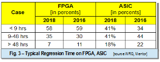
The typical regression time incurred by ASIC designs is longer compared with those of FPGA based as shown in the tabulated comparison using values extracted from the study. There is a notable increase (7%) in shorter ASIC regression taking less than 9 hours compared with 2016 data. On the other hand, FPGA regression taking longer than 9 hours seems to be on the increase (5%) compared with 2016 data.
Both FPGA and ASIC design teams have adopted similar dynamic techniques such as coverage metric based (code, functional), assertion and constrained random. On the static side, almost a third of ASIC designs have adopted formal property checking or verification, while FPGA is playing catch up as only about one-fifth of designs embraced the static techniques.
Most of the reported functional flaws are design error related, which is common root cause for both FPGA and ASIC. Likewise, verification engineers spend almost half of their verification time in doing debug (42-45%). One critical finding from 2018 study is the potential FPGA bugs rolled into production. 84% of FPGA design projects have non-trivial bugs escape into production as shown in figure 4.
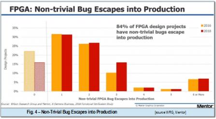
Key takeaways from this year study are ASIC projects displayed maturity in their processes while FPGA projects being pressured to catch-up in order to prevent bug escaping into production.
There are plenty of interesting data points which can be extracted from the study. For more details on 2018 Wilson Research Group Functional Verification Study, please check HERE.
Share this post via:


Comments
There are no comments yet.
You must register or log in to view/post comments.