
Each year, TSMC hosts two major events for customers – the Technology Symposium in the spring, and the Open Innovation Platform Ecosystem Forum in the fall. The Technology Symposium provides updates from TSMC on:
- (advanced) silicon process development status
- design enablement and EDA reference flow qualification
- (foundation, memory, and interface) IP availability
- advanced package offerings, and
- manufacturing capabilities and investments
A summary of the highlights from this earlier event is available here.
The OIP event provides a brief update from TSMC on these topics, and an opportunity for EDA vendors, IP providers, and end customers to highlight their progress (and their collaboration with TSMC) in addressing advanced process node requirements and challenges. This article offers a very subjective list of the Top 10 highlights of the TSMC 10th annual OIP Forum recently held in Santa Clara, CA.
(10) early engagement model with EDA partners and IP developers
TSMC provided an insightful chart depicting how their engagement model with IP developers has changed over the years, and the resulting acceleration of process introduction for new customer tapeouts (NTO).
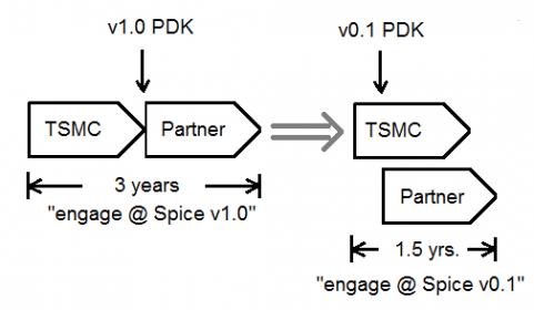
Leading-edge TSMC customers are now engaging at the PDK v0.1 level, providing an opportunity to “more fine tuning” and “improved design-technology optimization insights”, according to David Keller, President of TSMC North America.
This has enabled the time to PDK v1.0 process qualification and IP availability to be halved – more on the schedule for upcoming process nodes shortly. The risk, of course, is that early adopters must be extremely adept at evaluating and updating designs as the PDK data evolves, from v0.1 to v1.0 maturity. Nevertheless, kudos to TSMC for changing their engagement model and making the resource investment to accelerate advanced process design enablement release.
(9) TSMC, EDA vendors, and cloud services
There were multiple OIP presentations on the progress in support for transitioning design flows to cloud compute services, including end customer tapeout examples, cloud provider capabilities, and EDA vendors providing the “storefront” to the cloud resources (Cadence, Synopsys). There has clearly been significant progress in this area:
- data security
TSMC endorsed the security of these offerings, relative to their PDK and IP data.
- additional insights into the server core(s), memory, and classes of storage allocation appropriate for different EDA flows, for single-threaded, multi-threaded, and distributed execution
Yet, there remain additional areas of focus:
- accelerating cloud project “start-up” tasks
- optimizing the data communication requirements (and associated bandwidth) for transfer of design data and flow results between a customer’s host environment and the cloud services
- optimizing the allocated cloud compute/memory resources (versus throughput) for specific EDA flows
The presentation from the Microsoft Azure group referred to this opportunity as “cloud-native” and “born-in-the-cloud” EDA flow development.
- allocation and management of the customer’s EDA software licenses between on-premises and cloud execution
The cloud storefronts support either a dedicated license server hosted in the customer’s cloud chamber, or communication to an on-premises license server through a VPN.
In separate conversations, two colleagues of mine highlighted their key concerns:
“The insurance industry policies for cloud-based asset protection are not well understood.”
“I’m seeking new and more flexible software license allocation business terms with EDA vendors. The cloud allows me to quickly allocate compute servers for peak workloads, but I still need a full complement of (expensive) EDA licenses. I need to be convinced that the ROI to move projects to the cloud is substantial.”
(There was brief mention at OIP by one of the storefront providers of a “burst licensing” business model, but I did not pursue getting additional details.)
(8) N22ULP/N22ULL
The N22 node offers a “half-node” process shrink from N28 (i.e., N28 designs are directly subjected to an optical layout shrink).
All design kits and foundation IP for 22ULP are ready, with full interface IP availability scheduled for Q4’18.
Specifically, TSMC is focusing the 22ULL process offering on low leakage applications, both with the planar device Vt (Ion versus Ioff) options and with model development and IP characterization at low VDD (e.g., nominal VDD = 0.6V for 22ULL). A low leakage (EHVT) device will be available. The applications mentioned for 22ULL included low power microcontroller-based SoC designs and Bluetooth Low Energy (BLE) interface support, as would be common for IoT edge devices.
The 22ULL enablement will be staged in two phases – the v1.0 design kit for 0.8V VDD is released. The 0.6V VDD PDK and IP enablement will be available in June, 2019.
(7) Packaging
The diverse packaging technology offerings from TSMC continue to impress. The responsiveness to high-end customer requirements (e.g., CoWoS) and low-cost integration (e.g., Integrated FanOut, or InFO wafer-level fanout distribution) has provided unique differentiation. Briefly, the advanced offerings shown at OIP were:
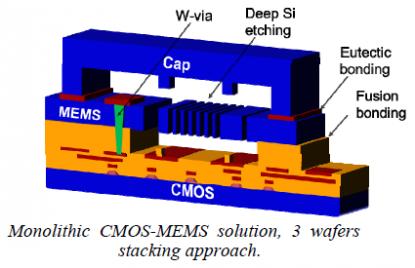
- wafer-level chip-scale packaging (WLCSP) integration
An description of a MEMS sensor (with cap) bonded to a CMOS die was provided — here is an example:
- InFO on Substrate
a hybrid of InFO and BGA design with multiple InFO die attached to a substrate carrier; 2/2um W/S interconnects between die; 40um microbump I/O pitch
- InFO with Memory on Substrate (qual. YE’18)
similar to InFO on Substrate, with an HBM memory die stack for one of the adjacent die
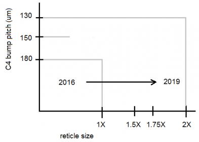
- CoWoS enhancements
both the C4 bump pitch and the reticle size (stitching) capabilities will be extended in 2019
- System on Integrated Chips (SoIC)
3D vertical stacking of multiple die, utilizing through silicon vias; design enablement in EDA flows in 1Q’19 (e.g., TSV-aware physical design, inter-die DRC/LVS, 3D coupling-based extraction, full SI/PI analysis)
(6) N7 and N7+ status
The transition from the production N7 node to the (partial, 4-layer EUV) N7+ offering is well underway. All EDA reference flows have been fully validated for N7+ to the v1.0 PDK. All foundation IP has been silicon-validated. The design kit for IP developers is available, and new tapeouts for N7+ are being accepted.
N7+ offers a 1.18X area benefit over N7, primarily due to a tighter metal pitch, and standard cell template support for a “common poly-on-device edge” (CPODE) isolation device between cells. To leverage the density gains of N7+ over N7 thus requires IP redesign – TSMC offers layout migration aids to assist with this transition.
Note that cell pin shapes may be allowed to violate minimum metal area lithography design rules, with the EDA requirements that pin cell area “patching” be incorporated into physical implementation flows. This will require changes to electromigration analysis, as well – the cell pin shapes will need to be promoted (and merged with the patch fill) to provide the extracted model for signal EM analysis.
(5) N5 enablement
The schedule for process node N5 design enablement was presented by Cliff Hou, TSMC VP for Technology Development:
- v0.5 PDK available, IP design underway
- TSMC foundation IP validated in silicon (e.g., standard cells, SRAM, eFuse)
- v0.9 PDK available in November, 2018
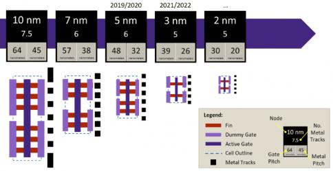
N5 represents the “full” EUV process introduction (e.g., 14 masks), with a 1.86X area shrink over N7.
Frequent Semiwiki readers will be aware of the challenges (and ongoing advances) for the transition to EUV lithography – e.g., source power, source uptime, statistical variation of exposure dose, resist sensitivity, mask blank defect density and mask inspection, pellicle technology. Interestingly, there was no indication at OIP that the N5 qualification schedule will be impacted by any of these EUV challenges.
(4) N5 unique EDA enablement features – part 1: 3:2 pitch ratio
The metal1 (vertical) to gate (vertical) pitch ratio in N5 is 3:2 – i.e., 3 M1 vertical tracks are equivalent to 2 gate pitch tracks.
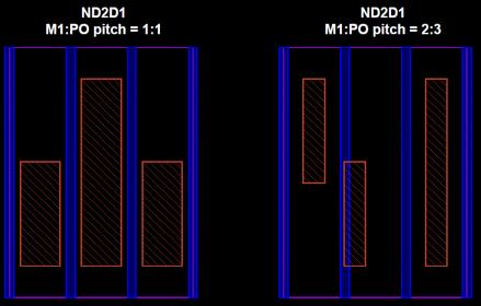
(Source: TSMC, L.C. Lu, ISPD 2017.)
Additionally, the M1 layer requires (full) multipatterning color assignment. This has necessitated unique cell design, cell placement restrictions, and routing requirements. As a Synopsys speaker noted, “One out of 4 sites is now legal for a cell – it used to be 98%.”
Electrically-equivalent (EEQ) cells are required in the cell library, to support track/color/pin shape alignment with the overall pitch grid.
Additional presentations highlighted examples of custom circuit designs requiring increased use of stacked n-high devices, and series-parallel mXn device stacks. The layouts for these device arrays need to adhere to the specific metal + poly grid pitch and coloring limitations mentioned above.
(3) N5 unique EDA enablement features – part 2: cross-row Vt rules
Traditionally, cell libraries included multiple variants, with different Vt selections for (nFET and/or pFET) devices within the logically-equivalent cell variants. Iterative cell swaps during power/performance optimizations could be performed, with (minor) limitations on inter-cell Vt selection within a row.
N5 introduces complex “cross-row” Vt rules, with EDA implications on: APR tools, power/perf. optimization, fill insertion, and (especially) ECO flows.
There is an increasing contribution due to “context-aware” device leakage – i.e., the device leakage currents within a cell are dependent upon the Vt type of neighboring cells. This implies a significant change to characterization flows. Cell characterization will need to utilize multiple surrounding layout context cells for accurate leakage modeling. Leakage “side file” models will be generated by characterization and read in during power_opt to select the specific context model corresponding to the actual physical layout.
(2) N5 unique design features – part 3: P/G design
The N5 power ground grid design for the standard cell template will differ significantly from previous nodes. A much higher density of M1 rails (+30%), with a correspondingly higher via count, will be required.
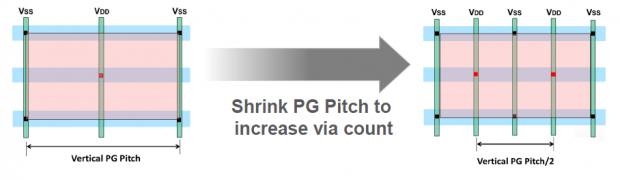
Note that a denser M1 P/G grid also impacts cell placement, as pin shapes will be blocked.
Also, to help alleviate the increasing issues at N5 associated with power distribution network dynamic voltage drop (DvD) due to higher resistivity, and to help address powerEM issues due to higher metal current density, TSMC is introducing a “super high-density” metal-insulator-metal (MIM) capacitive element for improved PDN decoupling. Insertion of these new MIM caps introduces complex routing rules in APR, and requires new parasitic extraction (and LVS) tool features.
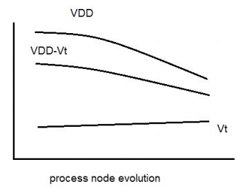
(1) N5 unique EDA enablement features – part 4: ultra-low voltage (ULV) delay modeling accuracy
Traditionally, cell arc delay models reflecting statistical process variation assumed a symmetrical Gaussian distribution (i.e., median = mean = mode). Statistical static timing analysis methods were applied to close timing and ensure robust circuit performance at “n-sigma”. Increasingly, advanced process nodes introduced asymmetric delay distributions, especially as the VDD supply was reduced more aggressively than design Vt (and thus, the (VDD-Vt) overdrive).
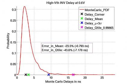
As a result, a “2nd generation” cell characterization variation format was introduced, supporting a distinct sigma for fast and slow delays on opposite sides of the distribution peak (mode).
At N5, the statistical delay distribution (at low VDD) is even more skewed, necessitating additional updates to the cell delay variation format – look for new characterization and Liberty Variation Format models to be introduced to reflect and additional “moment” of the distribution – namely, mean, sigma, and “skewness”. EDA SSTA tools will thus need to be enhanced in support of this new library model representation (link).
A compelling OIP presentation from TI highlighted the need for designers to focus on device aging mechanisms (e.g., HCI, BTI), and the resulting impact on circuit performance and EM robustness. The talk focused on the automotive market with TSMC 16FFC, but the fresh model-stress-aging model simulation flow (with self-heating acceleration) that was described would be generally applicable to any aging-based analysis.
Specifically, the comment that caught my attention was, “Selecting aging-related stress conditions can be extremely deceptive. Initially, we were primarily focused on evaluating worst-case performance paths with high-switching activity testcases. But, worst-case performance is not the same as worst-case aging. Hot carrier injection is usually associated with devices in saturation due to static DC biasing or switching transients. However, there may be devices in a quiescent sub-Vt condition – especially during extended periods of a power-down state – that are also subject to a high-stress environment. Consider an off device, perhaps in a device stack, which may be exposed to high Vds for an extended period. We found that “HCI-like” aging due to non-conductive stress can be a significant contribution to circuit parameter drift. identifying these cases requires insights from the designer to establish the aging simulation testcases, which may need to be uniquely developed separately from performance simulations.”
Sage advice, indeed.
There were several additional interesting topics discussed at OIP, especially by TSMC customers working to address the electrical challenges associated with N7 scaling:
- greater acceptance of “useful” clock skewing for timing closure and managing clock-related power transients
- new clock tree distribution topologies (hybrids of structured clock drivers with CTS-constructed trees)
- multi-pass routing (combining clock, critical signal NDR nets, and useful skew detailed routing)
- via pillar insertion for timing and EM optimization
Summary
The net of the TSMC OIP event was that N7+ and N5 process node development is progressing rapidly, with (apparently) little remaining technical obstacles to broad EUV introduction. There are new physical and electrical characteristics of N5 that impact cell design, APR, and cell characterization.
Reliability and aging flows will be increasingly critical, across all market segments.
TSMC continues to collaborate closely with customers on advanced packaging technology opportunities.
And, these advancements continue at a rapid pace, enabled by the TSMC OIP engagement model with EDA partners and IP developers.
-chipguy
Share this post via:


Comments
2 Replies to “Top 10 Highlights from the TSMC Open Innovation Platform Ecosystem Forum”
You must register or log in to view/post comments.