
Most people think that designing successful high speed analog circuits requires a mixture of magic, skill and lots of hard work. While this might be true, in reality it also requires a large dose of collaboration among each of the members of the design, tool and fabrication panoply. This point was recently made abundantly clear at the TSMC Open Innovation Platform (OIP) Forum held in Santa Clara on September 13th. Indeed, the entire OIP ecosystem was established by TSMC to encourage this kind of collaboration. Over the years it has enabled significant advances in electronic product design and delivery.
 Silicon Creations, a leading analog IP vendor, presented a paper this year at the OIP forum on their work with Mentor and TSMC in creating first time silicon success with PLL, SerDes and oscillator designs. The interesting part of this is that the technology they were working at is TSMC’s 7nm node. All of the difficulties of high speed analog design are amplified when working at 7nm. Because of the significant area and power advantages for digital designs, there is a compelling need for the supporting analog IP to enable completed chips.
In the paper presented by Randy Caplan, executive VP of Silicon Creations, and Mick Tegethoff, Director at Mentor, they provided an overview of the difficulties in design, modeling and simulation that the three companies faced and overcame to achieve working silicon. Silicon Creations provided the design development. TSMC provided silicon accurate models for the 7nm process. Mentor enabled the design flow with their Analog FastSPICE Platform. Mentor’s Calibre DRC/LVS/XACT-3D and PERC were used in the flow as well.
Silicon Creations has provided over 200 AMS IP designs since they were founded in 2006. These designs range from 350nm down to 7nm. This includes 170 different PLL designs. They have 9 PLL’s and oscillators on TSMC 7FF. They are on over 300 chips in production at TSMC. PLL’s turn out to be one of the highest volume analog IP’s. With over one billion instances, their PLLTS28HPMFRAC is used on 93 different production chips.
Silicon Creation’s SerDes range from <100Mbps to 20Gps, with very wide tuning ranges (up to 16:1) and random jitter less than 0.5ps RMS. The standards they support include PCIe, 10GKR, XAUI, SATA, V-by-1 HS, FastLVDS, CameraLink, FPDLink, RapidIO, OIF-CEI, JESD204, CPRI and semi-custom links. However, going to 7nm presents some new challenges.
Since 180nm, the number of GDS layers has increased by 5X. DRM size, a good indicator of process complexity, has grown 15X larger than it was for 35nm. With more rules and increasingly complex fill geometries, 7nm FinFET DRC runtimes have grown ~50X longer. In short the presenters assert that 7nm is quite complex and can be quite expensive.
Interconnect resistance is not just an issue for digital design. In analog designs at 7nm, wire resistance has a dramatic effect on performance. Consequently, extraction and simulation have become more complex, time consuming and critical. And, it turns out that there are more challenges for SPICE simulation of analog designs at 7nm.
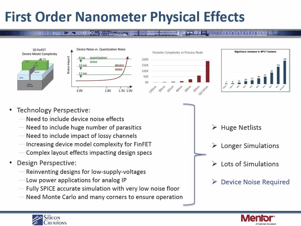
Traditional SPICE simulators are stressed by the demands resulting from more parastics and the need for more detailed modeling that includes variation, and device noise, among other things. Dynamic range must increase to over 100db. Simulations need to be run over long time intervals that capture PLL locking. And, driven circuitry needs to be included in runs to ensure proper system operation.
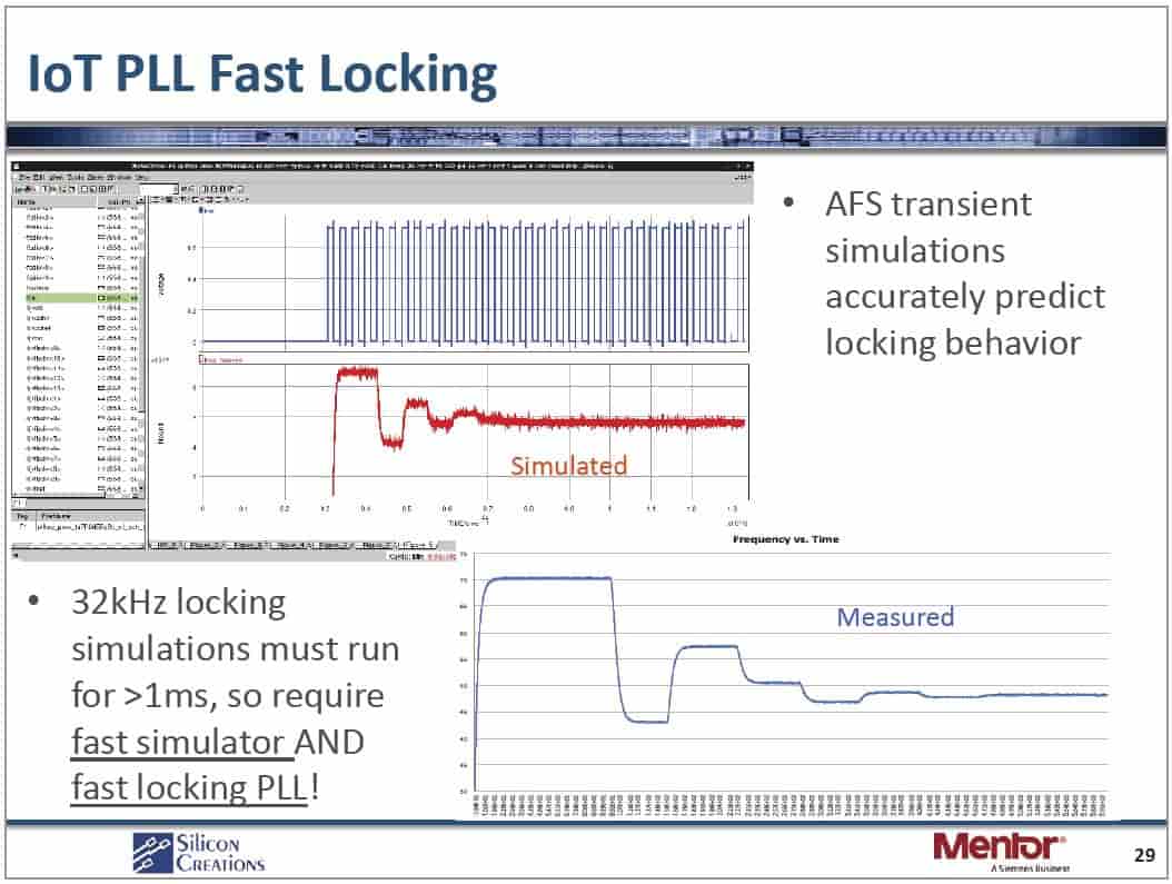
For their purposes Mentor’s AFS work extremely well. They were able to run simulations that predicted transient noise within 1-2db of silicon measurement data. They ran full spectrum periodic noise analysis that included all device noise sidebands and harmonics. This was using over 100K elements and they achieved PSS convergence. They also performed full spectrum oscillator noise analysis that included phase and amplitude noise.
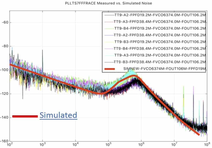
The presentation had a raft of data showing that over every performance metric that the analysis was extremely close to the measured silicon. And, most importantly the simulation coverage and runtimes were feasible for performing full design verification in a timely fashion. Speeding up the verification flow means more confidence at tape out and a higher likelihood of first silicon success, which was borne out by the results achieved after silicon came back from TSMC for all the designs run on their 7FF process. For a more detailed look at the specifics of this verification flow, refer to the white paper on the Silicon Creations’ web site.


Comments
There are no comments yet.
You must register or log in to view/post comments.