

 On September 6, 2017, Cadence Design Systems, Lumerical Solutions and PhoeniX Software hosted their second Photonics Summit. As with last year’s summit, this was a two-day event, with the first day including in a myriad of photonics presentations and the second day being a hands-on workshop. The hands-on workshop taught attendees how to use the Cadence, Lumerical and PhoeniX EPDA (electronic/photonic design automation) flow to put together a photonic system comprised of a photonic integrated circuit (PIC), a CMOS ASIC and a laser light source, all within a system-in-package (SiP) configuration using a silicon-based interposer.
While the hands-on day was very interesting I want to focus on the first day’s presentations. To paint with a broad brush, the overarching theme of the presentations seemed to be that there is an explosion in the breadth of photonics applications and the technology being applied across the entire photonic manufacturing ecosystem. Read on and you’ll see that integrated photonics is opening up applications that up till now have not been feasible with standard electronics.
In the past, I’ve told people that working on photonics is sort of like going back in time to the early IC days of the 1980’s. I now amend that premise. Instead, it’s like watching history repeat itself but on fast-forward. The progress shown and the number of people working the technology challenges is simply astounding. The collection of presenters at this year’s summit reflected this as they had presentations covering systems applications, wafer manufacturing and process design kits, packaging, automation for assembly and test and new design characterization Figures-of-Merit being applied to keep up with the dramatically increasing bandwidths made available through integrated photonics.
The first presentation was given by Andrew Wheeler of Hewlett Packard Enterprise (HPE) Labs, entitled ‘Photonics: the fabric of our (future) lives’. That’ a pretty bold statement when you think about it but Andrew unfolded a scenario that we are watching come true even as I post this article. Per Andrew, the amount of data we are processing is changing dramatically.
As a few examples, 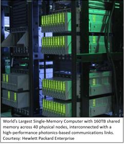 in 2016, Facebook members were posting an average of 4 Petabytes (PB) of data a day. That’s the equivalent of 4,000 Terabytes or 4,000,000 Gigabytes. In 2017, Walmart’s daily transaction database reached 40 PB and, in the not too far away future of 2020, it is estimated that automobiles employing driver assistance capabilities will generate around 40,000 PB daily! The advent of the internet-of-things (IoT) will exacerbate this further as we will have around 8 billion people on the planet using roughly 20 billion mobile devices to generate over 100 billion social infrastructure interactions per day using over 1 trillion apps.
HPE predicts that this data explosion will precipitate a massive change in the way we process data, moving from a processor-centric compute model to one that is a memory-driven compute model. Up till now, this has not been feasible due to bandwidth and latency limitations of electronics technology between processors and memory. Integrated photonics will change this as photonics interconnects eliminate the distance factor between processors and memory, facilitating entirely new compute topologies. It doesn’t stop there though. HPE also envisions photonic-based computing as opposed to simply using photonics as an interconnect fabric.
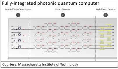 Along a similar vein, Darius Bunandar of MIT took photonic computing to a new level with a discussion how photonics enables Quantum computing. Photonics enables the creation of single photon sources and single-photon detectors which are the basic building blocks of Quantum computing. There is still much work to be done but the introduction of integrated photonics has already spawned more than a couple new startups in this space. Darius also gave another example of advanced photonic computing showing the realization of photonic-based deep neural networks (DNNs). These DNNs are the starting point of some very exciting work in artificial intelligence including image recognition and inferencing, running at the speed of light.
While this all sounds a little like science fiction, the rest of the speakers filled in the gaps for how these PICs will be manufactured, packaged, assembled and tested. Michael Rakowski from imec in Belgium gave an update on their silicon photonic processes that can now readily enable 50G NRZ photonic modulation and detection including how they are now tightly integrating CMOS ICs with PICs using 3D assembly techniques. These are the same techniques that were part of the Summit’s 2[SUP]nd[/SUP] day hands-on training session.
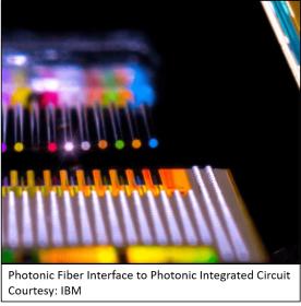
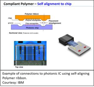 Paul Fortier of IBM followed with an excellent overview of automated high-throughput integrated photonics assembly capabilities. This presentation was especially interesting to see as one of the drawbacks for integrated photonics so far has been the cost of the PICs. Unlike electronic ICs, the packaging and assembly of photonics onto boards actually represents up to 80% of the overall cost of the PIC solution (just the inverse of electronics). Per Paul’s presentation, one of the key items now being developed is the ability to use existing electronic pick and place technology to assemble PICs on the boards. The tricky part here is that alignment must be precise for photonics to work correctly. IBM sees progress on three fronts, passive alignment of fiber arrays using v-groove technology, the use of self-aligning structures for polymer ribbon connectors and the use of flip-chip technologies that use solder-induced self-alignment. The common component in all of these is the idea of automated (hands-off) alignment of off-chip connections to the PIC.
Lastly, there were presentations from Dan Neugroschl of Chiral Photonics who work on photonics packaging and test and Pavel Zivny of Tektronix who works on tester and measurement equipment used for photonic testing. Not to beat a dead horse, but both Dan’s and Pavel’s presentations again showed how much infrastructural work has been going on to support integrated photonics. There’s probably two articles worth of information to share from those presentations that will need to wait for another day.
Suffice it to say, this summit turned out to be a very high-bandwidth presentation on the state of integrated silicon photonics. It was time well spent and I can’t wait to see what will transpire between now and the next summit.
If you are interested to learn more about what all of these gentlemen presented you can find their presentations at the link below.
See Also
Photonics Summit Proceedings
Cadence, Lumerical, PhoeniX Photonic Offering


Comments
There are no comments yet.
You must register or log in to view/post comments.