
 I had the pleasure of being able to attend the CDNLive event held in the Boston, MA area last month and I was pleasantly surprised to see that Cadence highlighted Silicon Photonics as one of its Keynote topics. MIT Professor Duane Boning gave an excellent overview of the current state of silicon photonics and why he believes it is time for the electrical engineering community to learn about this important technology. In Professor Boning’s presentation, he made the claim that silicon photonics has become “Interesting, Convergent and Designable”.
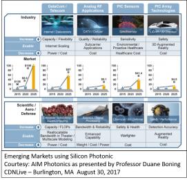 Professor Boning noted silicon photonics as interesting because it is bringing new functionality and capabilities to the market that are tied to real business. It is predicted that by the year 2025, the silicon photonics IC market will have reached $108 Billion with a little over half of that coming from the DataCom and Telecom industries. The data centers are pushing for greater bandwidth density while simultaneously desiring lower signal latency and lower overall power consumption. Silicon photonics technology gives them all three without compromise. Moving the photonic components from the active optical cables (AOCs) onto the server boards and eventually integrated with the processors themselves will drive IC volumes up dramatically. That will give the data centers the last important part of the equation, which is reduced cost. How many technologies give you more bandwidth density, less latency and less power consumption while also driving down costs?
The second biggest silicon photonics market will be in the area of sensors. This market is projected to grow to $41.4 billion by 2025. With the advent of the internet of things (IoT), sensors will be literally everywhere. One of the biggest drivers for volume ICs in sensing will be the healthcare industry where photonics will be combined with fluidics and electronics to deliver the long-awaited lab-on-a-chip. The lab will literally be brought to a patient’s bedside in the pocket of a technician. These ICs will be one-time use which means really high volumes and that will help to drive down IC costs. Sensing doesn’t stop at healthcare however. Sensors will also be heavily used in industrial and military applications as well.
One specialized form of sensor is used for imaging and will be especially useful for the autonomous vehicle market in the form of LIDAR (Light Detecting and Ranging). The market for LIDAR based imaging and display systems ICs is projected to reach $4.5 billion by 2025. Given all these applications it is no small wonder that Cadence Design Systems has hopped onto the photonics bandwagon.
The second thing Professor Boning noted was that silicon photonics is convergent. By that he explained that CMOS electronics and silicon-based photonics fabrication technologies have evolved toward each other to enable monolithic electro-photonic solutions.
There are currently two main approaches for monolithic integration. The first involves integrating photonics into the front-end-of-line (FEOL) layers while the second integrates photonics into the back-end-of-line (BEOL) layers. Both have their merits and their detractors. The good news is that no matter which way the industry goes, in both cases, photonics is sharing wafer processing, equipment and materials with standard CMOS. That means that silicon photonics can be added rapidly to commercial CMOS product lines with relatively low capital investment on the part of the foundries. We’ve already seen announcements from several of the production foundries adding silicon photonics to their offerings (Global Foundries, TowerJazz, TSMC/Luxtera, ST Microelectronics, and AMS).
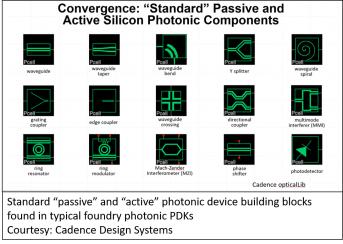 Also along the convergence path is the fact that photonics is mirroring electronics in its approach to design flow and design automation tools. The photonics ecosystem has been working for almost a decade now on establishing a common set of photonic device building blocks from which photonic circuits can be assembled. These building blocks are common in multiple foundry process design kits (PDKs) and can be used to design and map photonic circuits from one foundry to another through a process PhoeniX Software calls photonic synthesis.
Professor Boning also showed a slide of the recently announced Cadence, Lumerical, PhoeniX EPDA (electronic/photonic design automation) flow and noted that two of the break-out sessions presented at this CDNLive event were about the design and manufacturing of silicon photonics (courtesy Lumerical Solutions and Analog Photonics).
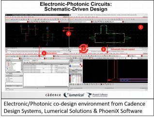 The last point Professor Boning made was that silicon photonics is now “designable”. As just mentioned, the design flow is mimicking that of electronics and now includes tools from multiple photonic and electronic design automation vendors. Design tools are now available for photonic device simulation, abstraction of photonic component behavior into compact models, photonic circuit simulation, automated layout generation including parameterized cells (pcells), DRC (design rule checking) and emerging LVS (layout vs schematic) flows. These tools and flows are supported by multiple foundries with qualified PDKs. More recently new flows for integration of digital and analog/mixed-signal electronics with photonic is now being put into place for systems-in-package (SiP) configurations (see Cadence Photonic Summit 2017).
For those interested in seeing where photonics is going and the kinds of capabilities that will be coming online in the next decade I refer you to the IPSR (Integrated Photonic Systems Roadmap) that can be found at http://photonicsmanufacturing.org/.
In summary, Cadence has done an excellent job of keeping their customers abreast of the latest evolving technologies and their CDNLive events are definitely worth attending. If you haven’t been to one in a while I would highly recommend you attend one to see what the world is up to. This one really shined some light (laser light that is) on the future.
See Also:
CDNLive website


Comments
0 Replies to “CDNLive Boston Keynote Address Highlights Emergence of Silicon Photonics”
You must register or log in to view/post comments.