

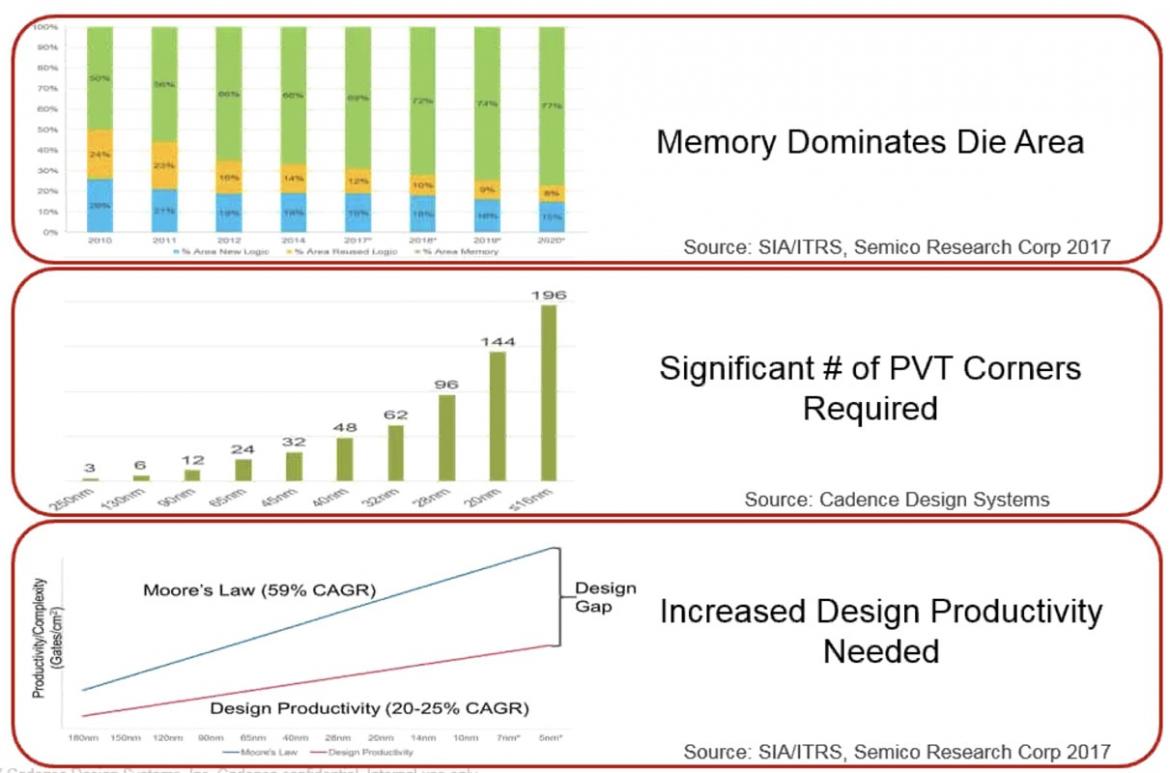
My IC design career started out with DRAM design, characterization and verification back in the 1970’s, so I vividly recall how much SPICE circuit simulation was involved, and how little automation we had back in the day, so we tended to cobble together our own scripts to help automate the process a bit. With each new process node offered the amount of SPICE circuit simulation for design and characterization has just increased caused by the number of PVT corners required, especially for IC designers doing memory IP. According to the SIA/ITRS many modern SoC designs can use up to 69% of their die area on memory IP blocks. At the 16nm process node we can expect to see some 196 PVT corners.
So today you still have a couple of choices for automating memory design tasks, either write your own automation scripts, or try something more integrated from an EDA vendor that knows the industry. The folks at Cadence scheduled a phone discussion with me earlier in September to provide an update on something new they had just finished working on that addresses this automation challenge. Cadence is calling this new tool flow Legato, and it’s focused on helping memory designers with three areas: Cell Design, Array and Compiler Verification, and Memory Characterization.
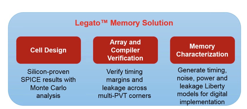
During the bit cell design phase circuit designers can perform variation analysis using Monte Carlo runs inside of the familiar Virtuoso environment, and the Spectre APSsimulator produces fast results using a parallel approach. Verifying instances of memory from an array compiler are best simulated with Spectre XPSbecause it’s a FastSPICE simulator with partitioning. Finally, to create all of the memory models (timing, power, signal integrity, current source) the Liberate tool is invoked and it simulates with Spectre XPS.
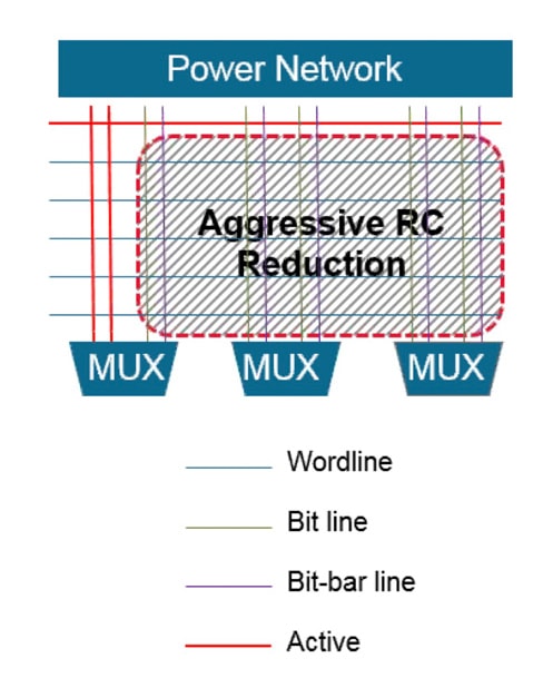
With Legato they’ve been able to speed up run times by 2X by using a variety of new techniques like RC reduction of parasitics on inactive bit and word lines:
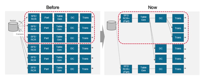
The process for simulating multiple PVT corners has been optimized by minimizing the partitioning steps and number of tables used by the FastSPICE circuit simulator, along with fewer DC operating points:
So Cadence has taken multiple point tools then re-engineered how they work in conjunction to optimize the overall run-time required during Memory design. The real proof is in what actual customers are doing with Legato, so from Yoshifurmi Okamoto at Socionext I learned:“Through our use of the Cadence Legato Memory Solution, we have experienced a 2X productivity gain when compared with our point solution and successfully taped out 12nm memory macro designs for our System-on-Chip solutions, and we can confirm good correlation between simulation result and silicon measurement.”
At Socionext they did a comparison of SRAM characterization for a 512×32 array on an 10LPE process node using point tools, then using Legato:
- 720,988 seconds, point tool
- 262,923 seconds, Legato
- 2.6X speedup with Legato
Summary
For memory IP designers using Cadence tools like Virtuoso, Spectre and Liberate, you now have something new in the EDA toolbox with Legato that will provide a 2X speed improvement at the same accuracy as before. This new, optimized flow is ready to go, so why not give it a try on your next project. Cadence acquired Altos Design Automation back in 2011 and over the past six years have continued to invest in this characterization tool, so they certainly understand the needs of this market.


Comments
There are no comments yet.
You must register or log in to view/post comments.