

I wrote up a quick article in the weeks before the Design Automation Conference (DAC) letting readers know that Integrated Photonics were indeed coming to DAC again this year. As a follow up, I attended the DAC presentation, ‘Capture the Light. An Integrated Photonics Design Solution from Cadence, Lumerical and PhoeniX Software’, given by Twan Korthorst, CEO of PhoeniX Software, at the Cadence Theater. Twan was also supported by Jonas Flueckiger of Lumerical Solutions as both PhoeniX and Lumerical are part of the overall Electronic Photonic Design Automation (EPDA) flow that uses Cadence’s Virtuoso system as the cockpit for the flow. The presentation was well attended with all seats at the theater filled. That, in and of itself, is significant given that the presentation started promptly at 10:00a when the exhibit floor doors opened for the day.
Twan started his presentation by setting context for how and where integrated photonics are emerging onto the scene. Photonics have been used for decades in long haul communications but it is now getting a new life driven firstly by the mega data centers. 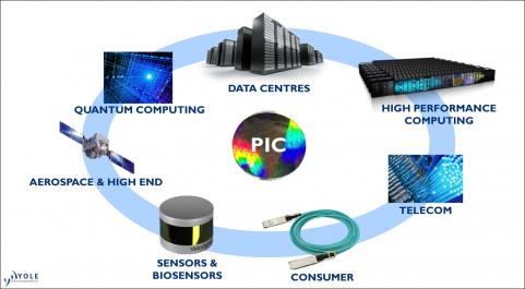 Active optical cables (AOCs) with integrated photonic ICs (PICs) are supplanting copper cables for the longer reaches required of the mega data centers. Photonics are also key to low cost, low energy 100Gbps connections now being installed in these centers. Additionally, integrated photonics are also finding their way into high performance computing, aerospace and high-end RF applications as well as sensors (both biosensors and environmental sensors). The advent of the Internet-of-Things with huge numbers of sensors may in fact be the real long-term high-volume driver for integrated photonics. Photonics is also a key enabler for quantum computing which is just now starting to emerge.
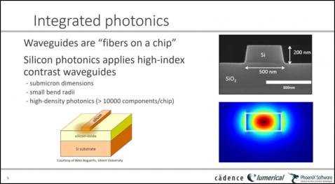
Twan also took the audience through a brief tutorial of what is meant by integrated photonics. In a nut shell, integrated photonics entails guiding laser light through waveguides on a chip (something akin to fibers on a chip). Chip manufacturing for integrated photonics comes in many flavors including Indium Phosphide, Silicon, Silicon Nitride and variations on other III-V compounds. The big interest now is in the use of silicon as a medium as it has the promise of leveraging the extensive manufacturing infrastructure already in place from more than 3 decades of CMOS processing. Silicon enables high-index contrast waveguides in sub-micron dimensions with small bend-radii. This translates into the capability to integrate tens of thousands of what were once expensive discreet optical components onto a single low-cost chip.
As mentioned earlier, Cadence, Lumerical and PhoeniX are now fielding a complete front-to-back EPDA flow and as is done in electronic design, the companies are leveraging the concept of process design kits (PDKs) 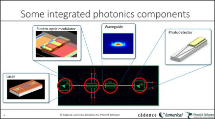 to enable designers to capture and connect their photonic circuit design using standard photonic building blocks and waveguides. At the simplest level, photonic components include lasers, electro-optic modulators, waveguides and photodetectors.
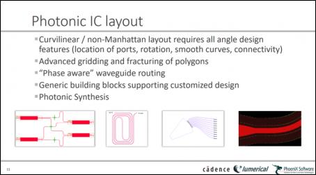
There are also components that are used to split, couple and switch light between waveguides as well as to multiplex/demultiplex multiple wavelengths of the light in to or out of waveguides. The new EPDA design flow enables co-design of electronics and photonics including schematic capture, co-simulation of electronics and photonics, schematic-driven layout of curvilinear photonic components and waveguides, back-annotation, design rule checking and GDSII generation complete with polygon discretization for different foundries.
The EPDA design flow is different from standard EDA flows in that it has added features to deal with the fact that photons do not behave the same as electrons. At 1550nm, the common wavelength used for the communications market, the design flow is akin to working with electronics that would be running at 193THz (that’s Tera-Hertz with a T). Photonics requires dedicated simulation routines that can accurately simulate the bidirectional propagation (including reflections) of the light while also comprehending that the light is multi-modal, in multiple frequency bands and accumulates phase shifts. In some cases, polarization is also comprehended and used. Photonics also requires smooth curvilinear bends in layout and as such requires specialized algorithms to deal with the generation of layout structures that will properly contain the modes of the light as it is manipulated throughout the circuit.
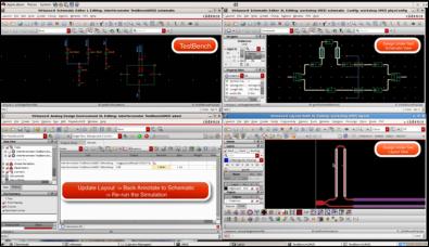
 As part of the presentation, Twan also ran a series of video snippets that showed the design flow in action, including co-simulation of electronics and photonics using Cadence’s Analog Design Environment (ADE) working in conjunction with Cadence’s Spectre spice simulator and Lumerical’s INTERCONNECT photonic circuit simulator. The companies have done a great job of integrating the tools as the test bench, stimulus and resulting waveforms were a natural extension of how analog electronic simulation is done today in the Cadence ADE flow. Similarly, video snippets were also shown for the layout portion of the flow where Virtuoso seamlessly called PhoeniX Software’s OptoDesigner product in the background to produce and manipulate all-angle curvilinear layouts without ever having to leave the Virtuoso layout GUI.
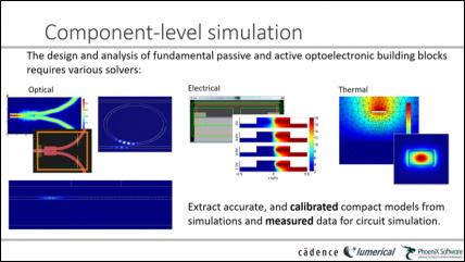
A step that was added for this demonstration was the addition of new interfaces between Cadence Virtuoso / PhoeniX layout and Lumerical’s component level simulation tools. These simulations include mode solvers, beam propagation and finite-difference time-domain (FDTD) algorithms that are used to model specific individual photonic components. The output of these simulations is used to create abstracted compact models that are used for the circuit level simulations that would be too large for component level algorithms.
Twan rounded out the presentation by announcing a two-day photonics summit that will be held at the Cadence campus in San Jose in early September. The event will include one day of technical presentations discussing the challenges and progress towards implementing integrated photonic systems for a variety of end applications. The event’s second day will include hands-on training of the EPDA framework and including a preview of how to do system design that combines electronic and photonic die with a laser using a photonic interposer, all within in a single package.
It’s always good to see new technologies come along as it means growth and new opportunities for both companies and individuals. Seeing integrated photonics at DAC is yet another sign that this technology is here to stay.
See also:
Cadence Photonics Solutions Web Page
Lumerical Solutions Web Page
PhoeniX Software Web Page


Comments
8 Replies to “Capture the Light with Integrated Photonics”
You must register or log in to view/post comments.