

Regular Semiwiki readers are aware of the rapid emergence of various (multi-die) advanced package technologies, such as: FOWLP (e.g., Amkor’s SWIFT, TSMC’s InFO); 2D die placement on a rigid substrate (e.g., TSMC’s CoWoS); and, 2.5D “stacked die” with vertical vias (e.g., any of the High Bandwidth Memory, or HBM, implementations).
Typically, one or more SoC’s are under development concurrently with the advanced package design. A vexing issue often arises, where the design platforms differ for chip and package, with different representations of system connectivity and circuit library models. As a result, there is no direct method for the SoC designer to build a correct connectivity model and simulate circuit paths between die (which potentially use different process PDK’s). Circuit validation throughout the multi-die package involves (error-prone) manual netlist creation, pulling data from the package environment into the circuit designer’s cockpit.
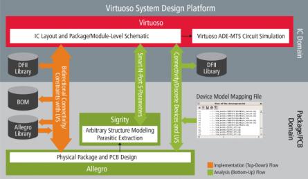
Cadence has recently addressed this flow deficiency, providing the necessary bridges between their leading Virtuoso and Allegro tool platforms.
I had the opportunity to chat with John Park, Product Management Director for IC Packaging and Cross-Platform Solutions at Cadence, about their new product, Virtuoso System Design Platform. “We have enhanced and extended Virtuoso. A product design team is able to incorporate a full-system hierarchical schematic model resident in Virtuoso SDP. We have developed a bi-directional bridge between the IC, package, and PCB design environments. There are two corresponding flows enabled by the Virtuoso SDP model – a new implementation flow and an analysis flow.”, John described.
The figure below provides an overall Cadence product architecture view, highlighting how Virtuoso System Design Platform provides the SoC designer with access to system connectivity and board/package parasitic data.
Virtuoso SDP Implementation Flow
As illustrated in the figure below, the implementation flow is invoked to automatically generate the die model data from Virtuoso SDP for use in Allegro SiP for package design – e.g., the schematic symbol, die physical footprint. In this example, three active SoC designs are underway – all the package (passive) components are represented in SDP, as well. Virtuoso SDP eliminates the issues associated with system connectivity data residing in different platforms and formats.
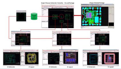
The SDP implementation flow generates the model exchange data between the Virtuoso and Allegro platforms, potentially on different operating systems – the “generate AllegroDB” operation imports the library and connectivity model into Allegro. The Virtuoso SDP cockpit is also used to maintain the techfile data used by Allegro – e.g., layer stackups, specific net implementation constraints. The SDP implementation flow provides the connectivity to verify the package/board LVS in Allegro (and for the connectivity use when building simulation models for analysis, discussed next).
Signal Integrity and Power Integrity Analysis
The analysis flow developed with the Virtuoso SDP offering provides several key validation features. The Sigrity family of signal integrity and power integrity tools is integrated into Virtuoso SDP.
Circuit Simulation
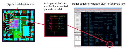
Additionally, SoC designers can use Sigrity to extract/connect complex multi-port Touchstone (S-parameter) model parasitics into a detailed die-package-die simulation in Cadence ADE (Spectre) invoked from the SDP cockpit GUI. The figure below illustrates the extraction of a model by Sigrity (a selected set of nets to generate a multi-port model), followed by the creation of a Virtuoso SDP instance that can then be used in die-package-die simulation.
Cadence has extended their Virtuoso platform to provide a unified cockpit for design teams to capture a system connectivity model. Additionally, implementation flow features are provided to generate the library, netlist, and design constraint data for advanced package and PCB design, to enable LVS connectivity verification in Allegro. The Sigrity model extraction features are integrated as well, for designers to run circuit analysis simulations. These features eliminate the tedious and error-prone tasks of constructing end-to-end circuit path models from disparate environments.
For additional information on the Cadence Virtuoso System Design Platform, please follow thislink.
-chipguy
Share this post via:


Comments
There are no comments yet.
You must register or log in to view/post comments.