

Since the beginning of time, people on Earth have peered into the night sky, pondering if they were alone in the universe. Today, we have a large group of scientists that are working to answer that question. The precision required for their search often depends on the performance of a key piece of technology – the analog-to-digital converter (ADC).
The ADC must meet exacting demands in differential linearity and dynamic range in order to be suitable for ground-based telescopes. Add to that low power demands (<1.5mW) for space telescope use and you have almost impossible requirements. The ADC must process faint signals from the imaging detector and without adding significant noise, map them into digital information that cosmologists use to piece together views of the universe.
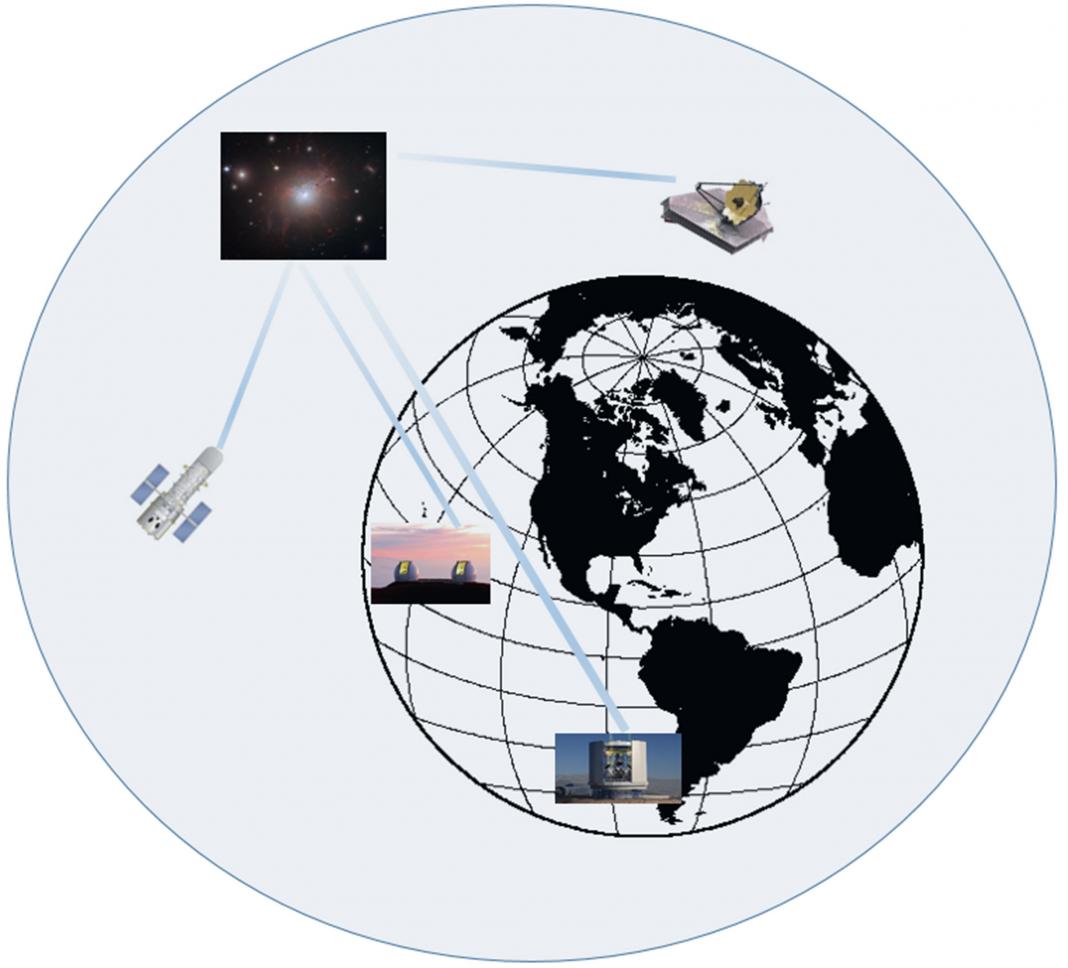
Lewyn Consulting Inc. (LCI) designed an x36, 19-bit ADC array that is part of the Teledyne SIDECAR (System for Image Digitization, Enhancement, Control, and Retrieval) ASIC. This ASIC is currently aboard the Hubble Space Telescope (HST), processing all the images from the Advanced Camera for Surveys (ACS). This ASIC is also on board the next-generation successor to the HST, the James Webb Space Telescope (JWST) scheduled to be launched in 2018.

A new class of very large ground-based telescopes are presently in operation or are in the planning stages of development. Several are in Chile including the Gemini South 8.1m telescope, the University of Tokyo Atacama Observatory (TAO) 6.5m telescope, and the Magellan 6.5m telescope pair (Baade and Clay). In addition, 2 telescopes are in Mauna Kea, Hawaii: the Subaru 8.2m telescope (at Mauna Kea, Hawaii) and the Keck 1 10m telescope. All of these telescopes have instruments that incorporate the LCI x36 ADC array in the Teledyne SIDECAR ASIC.
Images from the HST can trigger further exploration from these ground-based telescopes to research exoplanets in order to determine if they are capable of sustaining life. One of the keys to finding planetary candidates for sustaining life is to determine if they lie in a so-called “goldilocks-like habitable zone” of possible orbits. In such a zone, parameters such as planetary temperatures, atmosphere, and liquid water could be within the range of values that are generally accepted to be favorable to lifeform evolution.
Development and Verification of the Next-Generation ADC for Ground and Space Observation
The LCI x36 ADC array was originally designed to meet low-power requirements for the JWST mission. A proprietary, successive approximation register (SAR) topology was selected to also meet the demanding constraints imposed by the < 0.5 differential nonlinearity (DNL) and +/- 2 integral nonlinearity (INL) specification. Unfortunately, while the SAR topology could easily meet the 1.5mw power specification, speed was limited to 100KSPS at that power level. And, the high-speed mode was limited to 1MSPS.
Next-generation ADC discussions with engineers responsible for the European-Extra Large Telescope (E-ELT) project at the European Organisation for Astronomical Research in the Southern Hemisphere (ESO) and discussions with NASA in the U.S., resulted in the requirement to increase the ADC basic sample rate to 1 MSPS and the high-speed sample rate to 10 MSPS, while keeping power levels to 1.5mw per ADC for space-based applications.
Achieving Portable Physical and Circuit Design
In order to meet all the requirements for the next-generation ADC, LCI developed a proprietary ‘pipeline-like’ 17-bit ADC architecture with the goal of achieving very high speeds at power levels much lower than conventional pipeline ADCs operating at the same technology node. The use of portable physical design in the Tanner L-Edit layout editor and dimensionless circuit schematics created in Mentor’s Xpedition® DxDesigner, has allowed LCI to design one ADC that fits all of the requirements and it is portable from 250nm to 28nm for very-high speed (1 to 4 GSPS) operation. Sixteen-bit operation at 4 GSPS is accommodated using a 4-leaf structure with a common 4-phase clock.

Severe lithography pattern fidelity problems in the technology nodes smaller than 90nm drove new layout patterns for precise capacitors, precision resistor dividers, and CMOS devices. Current density limits for very high speed NMOS device wiring, vias, and contacts resulted in LCI not using standard PDK device patterns. To support these new layout patterns, LCI used the intuitive graphical editing features of L-Edit to control all the pattern-sensitive aspects of the structures.
Another layout challenge was how to implement the 2-color pattern decomposition required to improve lithographic pattern fidelity at 28nm and below. If layout geometries are not compatible with 2 or more color decomposition, computational lithography programs cannot proceed to completion during the mask-making process. To accommodate the physical design constraints to achieve correct 2-color decomposition, the layout was performed by hand using L-Edit.
Verifying the Physical Design
Because the next-generation LCI ADC has targeted rapid portability from 250nm to 28nm, it is essential that the both electrical and physical design be robust at all nodes (but especially at 28nm). To implement LVS in dimensionless Gamma units, LCI created a custom LVS-extraction command file by writing approximately 500 lines of code using Tanner Calibre® One whose nmLVS™ has the ability to use standard Calibre commands for layout parameter extraction.
For the ADC to be truly portable from 250nm to 28nm, several physical design verification tools were required to overcome the lithographic pattern fidelity problems at nanoscale technology nodes. It is well known that beyond 90nm, DRC-correct is no longer an assurance of high yields, especially for precision analog CMOS circuits. For example, metal layout patterns that do not violate metal width and spacing rules might still have dishing-related yield problems. Conversely, some metal patterns that violate metal width and spacing rules might not have dishing-related yield problems. The solution to deep-nanoscale DRC was to use Tanner Calibre One’s equation-based DRC tool (nmDRC™). This tool can determine which structures will yield and which ones won’t, and then report the results (even for metal patterns that violate formal spacing rules) in a way that is accepted by most foundries.
Verifying the Circuit Design
A common technique that CMOS designers use to verify design functionality is to set up and retain a number of testbenches that run various types of simulations such as DC operating point, AC/noise analysis, and gain/phase/bandwidth checks. With the number of sub-circuits exceeding 300 in a nanoscale, high-resolution pipeline ADC, the problem of keeping track of many different types of circuits used in different modules, and with different requirements (depending on placement in stage MDAC significance) can be overwhelming. To add to the problem, when different designers are working on different sub-blocks, the question of what changes are being made and what is the impact on the overall circuit performance adds a dimension of complexity that requires constantly re-running simulation and analyzing the results to ensure that the blocks still pass specifications. Tanner Designer helps the team track analog verification throughout the entire design cycle.
Tanner Designer is easy to set up to track and aggregate all simulation measurements for a project. The tool presents a dashboard that every team member can use to monitor the analog verification progress over the entire lifecycle of the design and verification process. If changes are made to any of the circuit components, designers can quickly rerun specified simulations and verify in the dashboard if all affected blocks still pass specifications.
Simulation measurement results can also be imported to a Microsoft® Excel® spreadsheet which allows the insertion of various mathematical functions developed by the designers to determine the quality of the result. For the ADC project, an Excel spreadsheet was used to calculate typical ADC characteristics such as integral nonlinearity (INL) and differential nonlinearity (DNL).
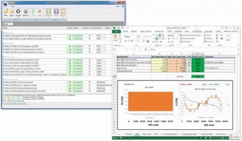
The Tanner Designer dashboard also manages every critical simulation required to verify final ADC performance. It identifies a number of critical simulations to be performed by circuit name and type. The dashboard lets designers interact with the schematic, view waveforms, and re-run one or more simulations. Tanner Designer also reports when all measurements for each simulation passes or fails specifications using custom information entered in the Excel spreadsheet that tracks all the measurements. The significant benefit of this dashboard is to keep all of the simulation results and master control in one place. Local control by the sub-circuit designer is also available.
Conclusion
We seek life on the exoplanets using space and ground telescopes with state-of-the art instruments. But, we need significantly higher-performance electronics to process the analog signals with higher precision and higher speeds for the larger detector arrays. LCI designed the next-generation of ultra-low power 17-bit ADCs with speeds that are 10x greater than achieved by the ADCs embedded in the Teledyne SIDECAR ASIC. LCI welcomes the continued development of the Mentor Graphics toolset to support design and verification in the next generation of IC fabrication technologies from FinFET at 15nm, to gate all around (GAA or NW) at 7nm, and beyond.
To learn more about the search for E.T. and how Dr. Lewyn designed the advanced ADC, see this whitepaper.
Dr. Lanny Lewyn, Founder, Lewyn Consulting Inc.
Nicolas Williams, Product Marketing Manager, Mentor Graphics


Comments
There are no comments yet.
You must register or log in to view/post comments.