

In constant pursuit of improved performance, power and cost, chip and system designers always want to 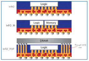 integrate more functions together because this minimizes inter-device loads (affecting performance and power) and bill of materials on the board (affecting cost). However it generally isn’t possible to integrate everything onto one piece of silicon; digital, RF, memory and sensor functions typically must be built using incompatible processes and often depend on isolation from other functions. So product teams have turned to advanced packaging options in which multiple die, potentially built in different processes, can be integrated within a package. This still reduces inter-die loads significantly and still results in a single device at the board level.
Among the best-known approaches, 2.5D and 3D packaging are particularly popular for memory, FPGA and CPU/GPU applications. But another related packaging methodology, Fanout Wafer-Level Packaging (burdened with the unappealing abbreviation FOWLP) is already seeing wider adoption in automotive, RF and mobile applications (as seen in recent iPhones).
Avoiding the gory details, the essence of FOWLP is to embed die side-by-side in an epoxy mold compound with IO pads exposed; routing distribution layers (RDLs) are then grown over the exposed faces to connect die together, and to connect to locations for external IOs. TSVs and traditional interposers are not required, which reduces cost and allows for thinner packages.
This might be no more than an interesting alternative for packaging were it not for the fact that TSMC (among other foundries) now offers an integrated FOWLP solution they call Integrated Fanout or InFO (a much more appealing abbreviation). You can fab die with TSMC and you can integrate them into an InFO package also with TSMC. This contrasts with FOWLP solutions offered by out-sourced assembly and test (OSAT) companies who obviously do not fab die themselves.
OSATs provide features that integrated foundry solutions do not (such as integrating die from multiple foundries) but with multiple suppliers in a package customers are ultimately responsible for managing yield issues. However, with an integrated solution like InFO and sufficient market muscle to force partner die providers to fab at TSMC, managing yield should be more tractable. As a friend once told me, it’s good to have just one throat to choke when you run into problems.
Which brings me to the EDA tooling you need to design this kind of integration. FOWLP packaging methods blur the line between die design (using Linux-based design tools with all kinds of disciplined design and verification automation) and package design (usually PC-based and driven more by expert judgment than automation). More information must be communicated between package designers and chip designers and it is increasingly common to expect some level of co-design between these two, to optimize die pinouts and power distribution networks for example. Analysis at the package level must also be much more comprehensive, considering electromigration, thermal, stress and warping effects, requiring more comprehensive analysis than commonly expected in package design.
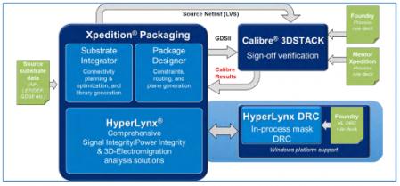
Mentor offers a very complete flow covering both design and signoff verification of FOWLP systems, starting with the Xpedition Package integrator. In conventional PCB applications Xpedition helps IC, packaging, and printed circuit board (PCB) co-design teams visualize and optimize complex single or multi-chip packages integrating silicon on board platforms. In FOWLP flows, the platform offers a single layout tool supporting fan-out as well as PCB, MCM, silicon photonics, RF and BGA designs. Users can drive rule-based I/O-level optimization and perform pin and ball-out studies from their respective domains, visualizing the impact across the complete system.
Electrical modeling and analysis of the package (die, package, substrate, board, etc.) is provided by Mentor’s HyperLynx simulation software. This analyzes design rule checks, power and signal integrity, EM, EMI and thermal; it also provides package model creation for use at the PCB level.
All of that is very necessary to design the integration but how do you get to a concept of signoff in these flows? Yields can’t be guaranteed or improved unless there is some kind of contract between customer and packager. In the IC world, this is accomplished through process design kits (PDKs). The customer signs off a design based on a PDK and the foundry guarantees their performance based on that signoff.
Mentor has introduced an approach for sign-off quality physical verification of packages which they call an assembly design kit (ADK). The purpose is similar to a PDK—to enable a contract for manufacturability and performance. What makes that happen, in both PDKs and ADKs, are standardized rules that ensure consistency across a process, qualified tool flows, interface formats, input/output formats—in short, everything a designer needs for successful design, tested and qualified and proven to produce working products. In one sense the ADK concept is not new. OSATs are already providing rules and tools for their own solutions. But the Mentor approach offers the hope of standardized requirements definitions, usable by OSAT and foundry providers and by EDA tool providers, just like we now expect for PDKs.
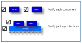
The platform to implement those signoff checks is the Calibre 3DSTACK functionality in Calibre nmPlatform. This is not just the IC Calibre you know and love, since it has to deal with a much more complex verification space. It requires a better understanding of the z-dimension than required for IC design. It has to deal with non-Manhattan shapes common in package design. And it must understand a wider range of formats such as ODB++ and comma-separated values for package netlists. Given these capabilities, package DRCs, package LVS, and interface checks can all be combined into a single Calibre 3DSTACK deck and checked in one run. The only individual runs required are for die-specific DRCs and LVS.
Calibre 3DSTACK is designed to support FOWLP designs for OSATs and foundries through ability to express die-by-die and package layer characteristics and rules. This is a big topic for which there’s a lot more detail than I have room (or expertise) to cover here. I recommend you read the more detailed white paper from Mentor to get a better understanding of capabilities and requirements.
Share this post via:


Comments
There are no comments yet.
You must register or log in to view/post comments.