
Imagine how semiconductor design sizes leapt higher with automation in digital design, which started from standard hardware languages like Verilog and VHDL; analog design automation is still catching up. However, it was not without a significant effort put in moving designers from entering schematics to writing RTL, which could be automatically verified and synthesized to gate level netlist.
Today, the designs have grown bigger and more complex with a complete system appearing on a chip. It’s a tedious task writing RTL for a complete chip and verifying it with a single verification approach. Design and verification productivity is at stake, which needs urgent improvement through change in design methodologies.
Higher levels of abstractions are possible where the system can be described in higher level languages like ‘C’ or SystemC, which can be simulated several hundred times faster than RTL. This provides a great opportunity for a quick architectural exploration at the top level for best PPA (Power, Performance, and Area) with the least investment of resources and time. This novel approach is taking longer than expected in its proliferation across the semiconductor design industry. However, there are promising tools and methodologies, which are being adopted by leading SoC and IP design companies and are being deployed in their standard design flows. Let’s review how this is being done and what more needs to be done to bring this approach in the main stream of SoC design and verification.
Qualcomm, the largest fabless semiconductor company has established a standardized high-level synthesis (HLS) and high-level verification (HLV) based design flow throughout the company. The flow has been successfully used in several image processing, video processing and other IP of different complexities; and chips taped out using those IP. This is an outcome of Qualcomm’s multi-year work with Calypto (now Mentor Graphics). Qualcomm also presented about their HLS/HLV based methodology in the 52[SUP]nd[/SUP] DAC.

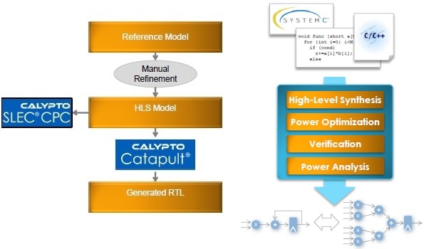
Mentor’s Catapult[SUP]®[/SUP] 8synthesizes C++/ SystemC into an optimized RTL. Testing the synthesizable C++/SystemC catches bugs more quickly, because the code simulates hundreds of times faster and is typically 1/5[SUP]th[/SUP] the number of lines of comparable RTL. Much less debugging is then needed on the generated RTL, which accelerates verification downstream and reduces the total verification time by half. The RTL is also power optimized through Mentor’s PowerPro[SUP]®[/SUP] optimization and analysis technology under the hood in Catapult 8. The verification starts very early in the design cycle. The reference model in C/C++ is refined and then cleaned through SLEC[SUP]®[/SUP] CPC, the C property checking tool, which detects all static errors in the code and also checks the assertions and cover points set by the user. The HLS model thus produced is easily synthesized into an optimized and correct RTL that can easily go through the downstream design flow. Also SLEC (Sequential Equivalence Logic Checker) can formally verify the generated RTL against the source C/C++.
A homogeneous system in C/C++ provides quick and extensive architectural exploration and verification closure through HLS/HLV methodology. The test infrastructure used during HLV can be reused during RTL verification, thus improving the productivity of downstream verification flow as well.
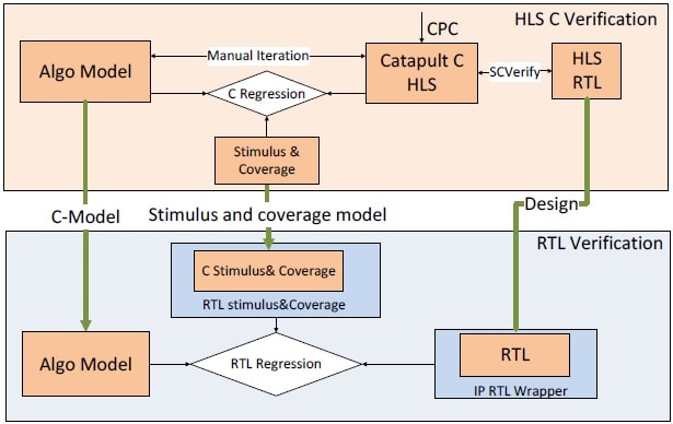
Starting with an algorithm, the architecture can be appropriately divided between hardware and software. The hardware can be modelled further into synthesizable and non-synthesizable ‘C’. The algorithmic hardware model thus created is synthesized using Catapult HLS tool and verified in ‘C’. The ‘C’ regression thus created can be complemented with RTL regression during RTL verification.
By making small changes in the code of algorithmic model or in the constraints on the synthesis tool, one can quickly generate new design architecture and compare it with the older ones. This provides an opportunity to quickly iterate over several architectures and determine the best architecture for a design. Also the designs with different power profiles can be reviewed with this approach, which is not possible with traditional RTL flow because power data becomes available very late in the design cycle.
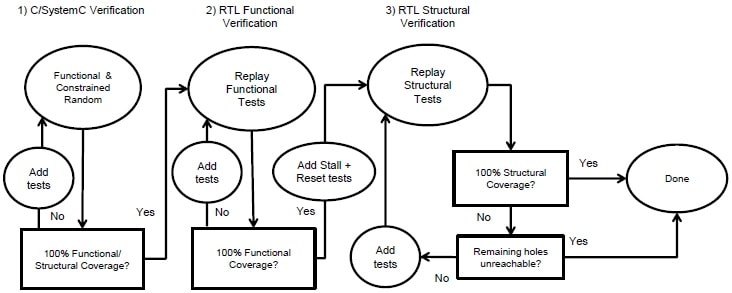
Complete verification coverage can be attained in 3 stages; 100% functional/structural coverage during C/SystemC verification, 100% functional coverage during RTL functional verification, and complete structural coverage during RTL structural verification. Any uncovered hole must be determined to be unreachable.
Qualcomm has used an established C codebase for certain designs by simply changing the target library for technologies ranging from 65nm to 14nm. The enhancements and new features can be easily added onto that codebase. It’s clear that the ECO flow is quite fast and efficient. So, the changes can be done quite late in a design cycle.
Well, HLS/HLV methodology works very efficiently at a higher level (C/C++/SystemC) and complements very well with the downstream RTL flow. However, design signoff still takes place at RTL and gate level due to limitations in current HLS toolset and methodology, which works mostly with algorithmic models at IP level.
While talking with Bryan Bowyer, Director of Engineering at Calypto Systems Division of Mentor Graphics, I learnt that they are working with partners to make SLEC more generic to check equivalence between ‘C’ and RTL. Also, Mentor is driving an effort going on in Accellera SystemC Synthesis Working Group to standardize HLS flow through a common synthesizable subset of SystemC across the industry.
The way design signoff has moved up from gate to RTL level today, we hope the signoff moves further up to ‘C’ or SystemC level in future.
For more details on Qualcomm’s HLS/HLV methodology, a whitepaper at Calypto’s website can be referred HERE.
Pawan Kumar Fangaria
Founder & President at www.fangarias.com


Comments
0 Replies to “Leveraging HLS/HLV Flow for ASIC Design Productivity”
You must register or log in to view/post comments.