
Electro Static Discharge (ESD) has been a major cause of failures in electronic devices. As the electronic devices have moved towards high density SoCs accommodating ever increasing number of gates at lower process nodes, their vulnerability to ESD effects has only increased. Among the reasons for ESD failures in SoCs, device breakdown and interconnect melt-down account for more than 70% of the overall ESD failures. Long term reliability is anyway at stake due to such ESD issues; they can even impact the first silicon success.

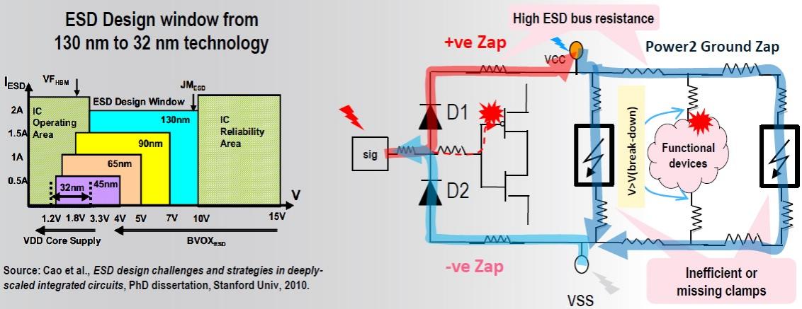
Look at how the ESD design window for MOS devices has shrunk as the technology node moved from 130nm to 32nm. The margin between operating voltage and oxide breakdown voltage has continued to decrease, making a device more prone to breakdown due to ESD. High current flow through unintended paths due to any kind of ESD effect (Human Body, Machine or Charged Device Model) can render the device to failure. To protect the devices from ESD, it’s important and essential to introduce effective clamp circuits with I/O and P/G pads that can handle large transient currents, provide efficient discharge paths to ESD currents and prevent any pin voltage from exceeding the oxide breakdown voltage.
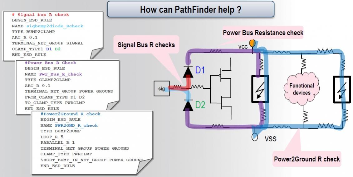
In aDAC 2014 presentation I found that PathFinder from ANSYS is a state-of-the-art tool that can precisely check the resistances of signal bus, power bus and the power-to-ground path to help designers appropriately plan protection circuits for device breakdown due to any ESD event.
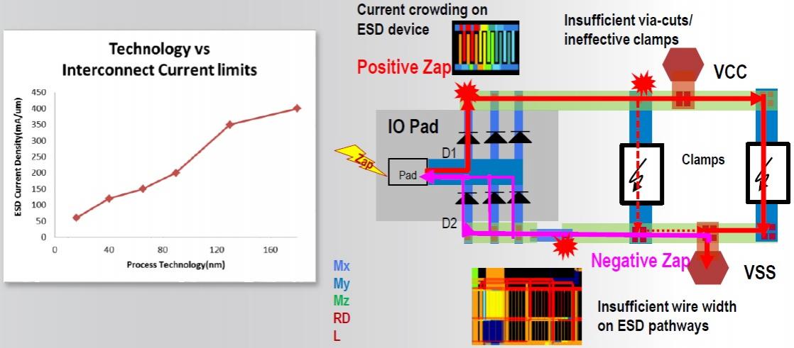
If we look at the interconnect scenario, that also has become extremely vulnerable at lower technology nodes with ESD current limits going down significantly. Any current crowding on ESD devices or insufficient wire width on ESD pathways can cause melting of associated interconnect. Appropriate signal and power buses and clamps needs to be planned to prevent interconnect melt-down.
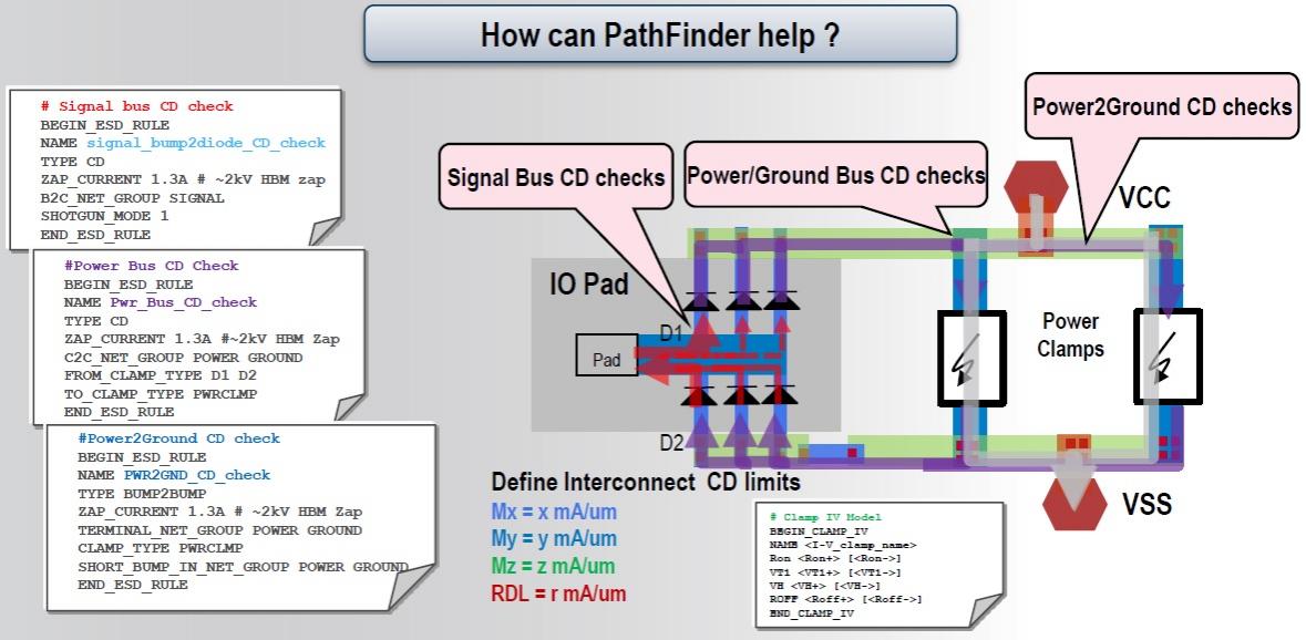
ANSYS PathFinder can precisely define CD limits for interconnect and check it for signal bus, power/ground bus, and the power-to-ground path, thus helping designers appropriately plan for the buses and power-to-ground paths and prevent their melt-down due to any ESD event.
Today, an SoC can have multiple IPs and blocks under different power domains. This also can give rise to cross-domain ESD issues if not properly analyzed and taken care of.
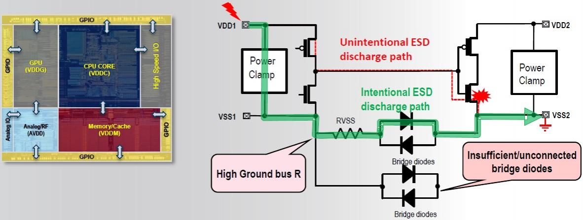
Above is an example where ESD discharge can pass through an unintentional path causing failure. The circuit must be analyzed for such eventualities and protected from ESD.
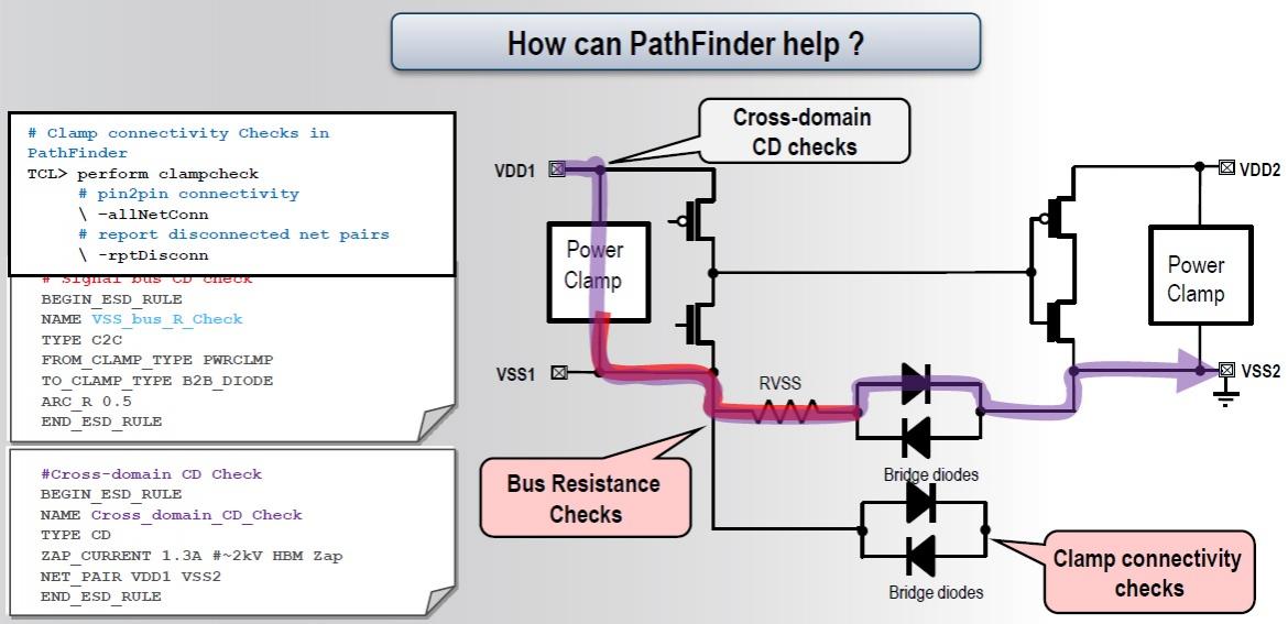
PathFinder performs cross-domain CD checks, bus resistance checks, and clamp connectivity checks to prevent such ESD issues that can arise at the boundaries of different domains.
Thus PathFinder provides a powerful solution for accurate ESD analysis and prevention of ESD issues in both, IP and SoCs. It takes layout, technology information, Spice netlist including clamp models, and ESD rules as inputs and then performs all kinds of checks including resistance check, interconnect failure check, layout connectivity check, and dynamic CDM checks for IPs. The PathFinder can be used from very early stages of a design such as I/O pad planning, I/O ring planning, and floorplanning until the final sign-off. It has very easy-to-use GUI for debugging and finding root causes of issues, and fixing those. The tool is robust enough with capacity to handle full-chip analysis including its package.
This ESD solution using PathFinder is part of ESDA(ESD Association) reference flow and TSMC reference flow.
Share this post via:


Comments
0 Replies to “SoCs More Vulnerable to ESD at Lower Nodes”
You must register or log in to view/post comments.