

We read about FinFET technology in the semiconductor press daily now, thanks to Intel introducing their TriGate transistors starting in 2011 and creating a race with foundries and IDMs to switch from planar CMOS nodes. To get some perspective about the progress of FinFET IP and EDA tools I spoke with two experts from Synopsys, Swami Venkat and Saleem Haider. Synopsys is an EDA software company that enables FinFET chips to be designed, verified and implemented. We spoke by phone on Friday, March 6th.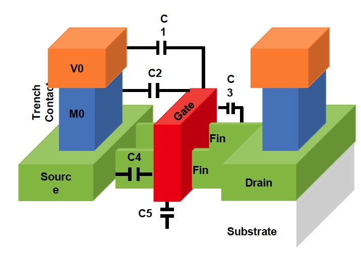 For the past three years 2012-2014, the general FinFET progression has been mostly test chips and limited production, outside of Intel. At DAC in June 2014 we saw the first 14 nm FinFET production silicon from Samsung. Intel now has a 2nd generation FinFET technology at 14 nm used in their Core M Processor.
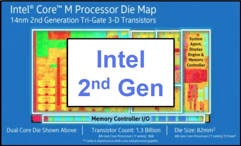 All new semiconductor process technologies start out with 3D TCAD tools that predict the physical and electrical properties, start to build up models used by SPICE circuit simulators, and create flows for parasitic extraction. Even IP development can start at this early stage, and for FinFET that process started back in 2005 with SPICE models.From 2012 to 2013 the commercial EDA tools were updated to work with FinFET requirements, and in the past two years the IP companies, foundries and IDMs have been validating their FinFET designs through test chips, correlating silicon to their models and announcing IP libraries. All of this groundwork now makes 2015 the year that FinFET designs are in production ramp up, like the Samsung Galaxy S6 phone announced this week. Early collaboration between foundry, IP and EDA companies was critical to the success of FinFET use.Related – What’s New with Static Timing AnalysisSynopsys EDA tools are FinFET ready and silicon is working:
- FinFET device modeling and circuit simulation: HSPICE, CustomSim, FineSim
- FinFET IC layout editing with abutment rule, double patterning, MEOL (Middle End of Line) layers: Laker Layout
- FinFET parasitic extraction: StarRC
- FinFET layout rule compliance for DRC (Design Rule Checking) and DPT (Double Patterning Technology): IC Validator
- Place and route with quantized rules, grid rules, optimizations: IC Compiler I, IC Compiler II
- Static Timing Analysis with waveform-propagation delay calculation: PrimeTime
Related – How Well is HSPICE Tracking Current Design Trends?Use of the Synopsys EDA tools are so popular that some 90% of volume production FinFET chips use at least one of their tools. These customers include:
- HiSilicon Technologies (ARM Cortex-A72, Cortex-A57, Cortex-A53 for wireless)
- Marvell
- Netronome
- NVIDIA
- Foundries
- Intel Custom Foundry (Achronix)
- GLOBALFOUNDRIES
- SAMSUNG
- TSMC
- Samsung
One EDA tool for Place & Route optimized for FinFET is IC Compiler II, announced about one year ago. Compared to the first generation IC Compiler tool you can expect a speed-up of 10X, and better QoR (Quality of Results), while using less RAM resources. With that speed improvement engineers can now consider doing more explorations to optimize for for area or frequency, while pulling in the schedule a bit.The IC Compiler II tool is now used at 27 different customers, with 67 engagements and 17 tape-outs so far. Adoption looks brisk for a relatively new tool, so that’s a good sign, plus there are several customers that have testimonials: ARM, Imagination, LSI, MediaTek, Panasonic, Renesas, ST Microelectronics, Samsung and Toshiba.Related – How Imagination tested the PowerVR Series6XTTrendsThe 20 nm planar node required DPT, which was more complex on implementation and the power, performance and area weren’t compelling enough. Many customers opted to skip the 20 nm node, and instead go to 16 nm and 14 nm FinFET instead.Chip speed as measured in GHz is increasing again with FinFET technology. Leakage on planar devices was limiting the GHz race. The pressure is on for dynamic power optimization, pushing P&R tools and improving QoR.FinFET at 16 nm and lower nodes the routing is now limiting the overall density, so having technology like Zroute helps meet routing requirements.The size of physical partitions must increase, so 100 blocks in a chip is happening today. Partitions with up to 5-10 million cells can now be handled.SummaryEDA companies, IP providers and foundries have created virtual teams that have closely collaborated to enable the FinFET revolution that we are now witnessing in production quantities for 2015. These are very exciting times for consumers like me, because I get to enjoy products that were unthinkable only a few years ago.
Share this post via:


Comments
0 Replies to “FinFET Design Enablement”
You must register or log in to view/post comments.