
In this age of SoCs with hundreds of IPs from different sources integrated together and working at high operating frequencies, FPGA designers are hard pressed keeping up the chip reliability from issues arising out of excessive static & dynamic IR drop, power & ground noise, electro migration and so on. While the IPs are tested and verified in isolation, their real test begins when all types of IPs (digital, analog, mixed-signal etc.) interface with each other and works together inside an SoC. An integrated analysis, verification and optimization methodology must exist, not only for the chip but also with package and board included, that can sign-off the system for power noise reliability as well as electro migration (EM).
Although the electrical concepts for verifying these appear to be simple, large design sizes with varying degrees of complexities including mixed-signal, multi-voltage, low noise margin etc. make the task a great challenge for designers. The static IR drop works on DC pattern (with average current); it is good to determine early gross weakness of the design but cannot represent true transient noise analysis. Dynamic transient analysis takes into account the actual leakage and transient switching currents. Typically the P/G network is extracted into RLC circuit and Spice level simulation is done for transient noise analysis. However, due to large size and complexity of RLC network, using Spice is not a viable alternative. Fast-Spice simulators have appeared, yet they may not be sufficient to complete the P/G analysis for large SoCs in a reasonable time and can have issues with their methodology in identifying IR and EM bottlenecks.
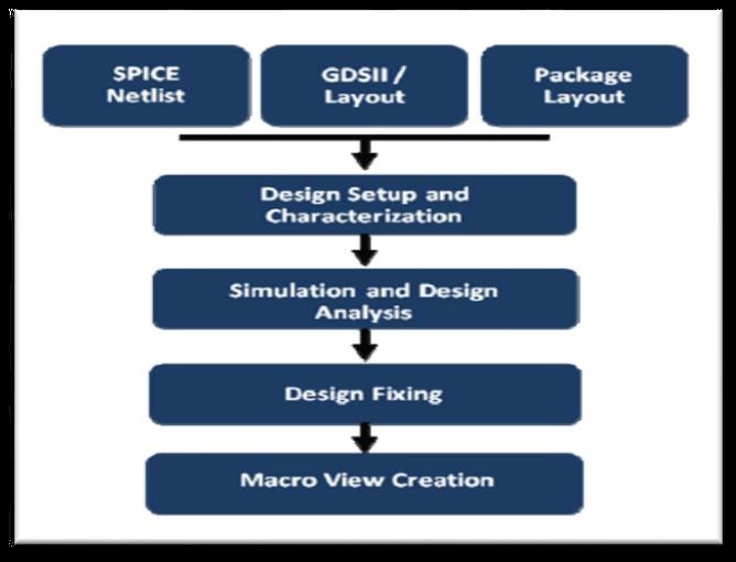
Xilinx has developed an integrated comprehensive single pass flow for static and dynamic voltage drop analysis both at IP as well as full-chip level. It uses Apache’sTotem and RedHawk platform for analysis and simulation.

[Static and Dynamic Voltage Drop Analysis Flow]
IP data is provided in GDSII layout, Spice netlist in DSPF/SPEF format, and testbench or input vectors in Spice format. For an IC or SoC, package layout is also needed. Also, technology parameters in industry standard format (iRCX, nxtgrd), device model data, and layer mapping information are required. Simulations are performed with pre-characterization and layout data; then analysis is done for any design weakness or hotspot. Interactive fixing and analysis are done to resolve issues and then a clean transistor level model is written out for full-chip level analysis. This flow is able to perform analysis for large IPs while maintaining Spice level accuracy by using several techniques.
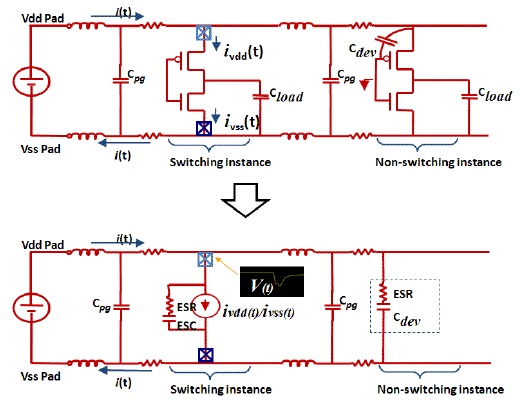
[Circuit Modeling Detail]
The non-linear nature of the circuit is transformed into linear by pre-characterizing the current, intrinsic resistance and device capacitance for each transistor and replacing every transistor by its own model. The RLC elements of P/G network and associated package/board are extracted and simulated for P/G noise in the circuit. The transistor models act as current sink while parasitic network provides the impedance. The capacitance can come from various sources such as P/G mesh, device diffusion and gate, signal line, and on chip. The linear circuit is then solved by proprietary solver technology and voltage/current can be obtained at every wire, via and transistor.
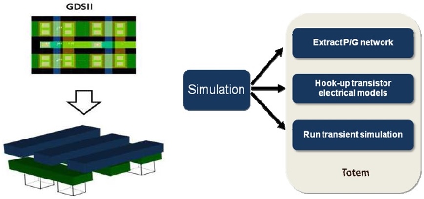
[GDSII Modeling and Simulation Flow Using Totem]
GDSIIdata is used to create model of the power and ground geometries along with the locations of transistors. A high performance & capacity RLC extraction engine (that exploits the regularity in P/G mesh) is used to obtain the parasitic of the P/G network for all power domains with selective inclusion of capacitance and inductance of the mesh as needed (not needed for static analysis).
For static analysis, an average or peak device current is used and the DC voltage/current is computed for each wire and via starting from the voltage sources to the transistors. For transient analysis, the true characterized transient current profile is used along with the associated effective transistor resistance and capacitances and time-domain current and voltage waveforms are computed for each wire and via.
The electro-migration for wires and vias is simultaneously determined based on the current flowing through the P/G mesh and violations checked against the limits defined in the technology file. For static analysis, DC or average EM limits are checked. For transient analysis, average, RMS and peak EM limits are checked.
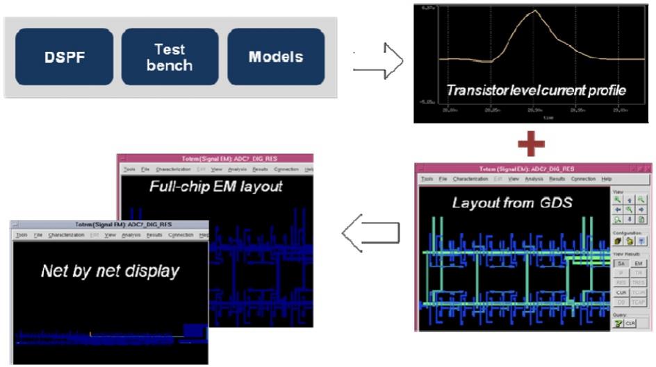
[Signal EM Analysis with Vectored Approach]
The signal interconnect EM is verified in a similar manner where switching currents for transistors connected to signal nets are pre-characterized and used to model the average, RMS and peak currents on a signal net and compared against the limits specified in the technology file. This can be done in vectored as well as vector-less approach. In vector-less approach, the current waveform at a driver output is constructed based on certain basic parameters provided for a net under analysis. The vector-less approach can be used to gain 100% coverage and be able to sign-off EM on each signal net in the semiconductor design.
By aligning with the bottom-up approach of FPGA designs where IPs are developed separately and integrated together, this methodology promotes IP reuse. The challenge is to perform IP level validation and then model top level connectivity with IP level design constraints such as maximum allowable voltage drop. The CMM blocks can be used for full-chip analysis of mixed-signal design without compromising accuracy and runtime.
More details of this methodology can be referred in a technical paperjointly authored by Sujeeth Udipi at Xilinx and Karan Sahni at Apache, and presented at DesignCon 2014.The paper also suggests about the type of analysis required for different types of design styles in order to save time without loss of accuracy.


More Articles by Pawan Fangaria…..
Share this post via:


Comments
There are no comments yet.
You must register or log in to view/post comments.