

One of the first blogs I wrote on SemiWiki was on clock domain crossing (CDC). I thought it was rather a specialized subject, a sort of minority interest. It turned out to be one of the most-read blogs I’ve written. Modern SoCs have lots of unrelated clocks, maybe hundreds, and so ensuring that signals going from one clock domain to another are correctly handled is not a minority interest at all, it is right in the mainstream. Design and verification teams spend a huge amount of time on verifying the correctness of asynchronous boundaries on the chip. Incorrect asynchronous boundaries can cause multiple design defects not encountered in traditional single-clock-domain designs.
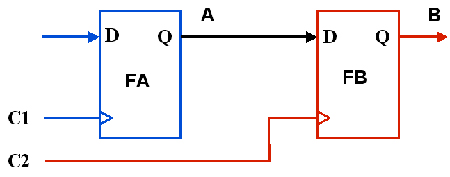
Metastability is one of the major defects. A flip-flop is metastable if its clock and data change very closely in time causing the output to be at an unknown logic value for an unbounded period of time. While metastability cannot be eliminated, it is usually tolerated by adding a multi-flop synchronizer to control asynchronous boundaries and using those synchronizers to block the destination of an asynchronous boundary when its source is changing. FIFOs, 2-phase and 4-phase handshakes are typical structures used for this type of synchronization.
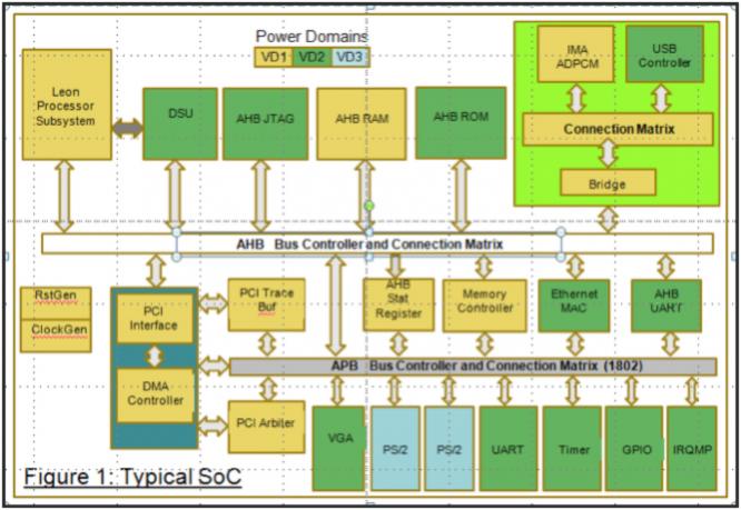
Glitches on asynchronous boundaries are the causes of defects as well. A glitch on an asynchronous crossing can cause the capture of an incorrect signal transition. Data coherency issues occur in a design when multiple synchronizers that have settled to their new values in different cycles interact in downstream logic. While the concepts and methodologies for verification of such issues have been extensively researched in the past ten years, little work has been attempted to tackle clock domain crossing (CDC) verification signoff of large system-on-chip (SoC) designs such as the design below.
There are three main methodologies used to verify CDC correctness:
- flat CDC verification
- hierarchical bottom-up CDC verification
- hierarchical top-down CDC verification
In flat CDC verification, the entire SoC is verified in a single run. Flat SoC verification covers all the critical issues I discussed earlier: metastability, glitches and loss of coherency in addition to functional requirements of the asynchronous interfaces and other critical issues across data, control, clock and reset circuitry. The size and complexity of a design is no excuse for missing a CDC bug. The main advantage of flat SoC verification is setup simplicity. Typically, clocks, modes and other design constraints are available at the chip level and therefore design setup for CDC verification is straightforward. The big problem, though, is that the whole chip is only put together late in the design cycle which means that errors that could have been caught early in the design cycle when there is slack in the schedule to fix them only get caught later when it is right on the critical path to tapeout.
In hierarchical bottom-up CDC verification, blocks are verified as they are completed. As blocks are assembled to build subsystems and finally the SoC, the verification is scaled to the subsystem or SoC level leveraging the information available from the verification of blocks previously verified. This approach finds problems early and is especially well-suited to distributed development where many of the blocks are developed in different groups from the group putting the whole SoC together, a typical way of working for modern semiconductor companies.
Sometimes, SoCs are developed in a top-down manner where top-level constraint are created very early in the design cycle and blocks are then developed and gradually integrated to complete the SoC design. In such a design flow the early availability of SoC constraints can be leveraged for effective top-down CDC verification. In other words, CDC verification can be applied to the top level SoC and the CDC issues can be associated with specific blocks, or with inter-block boundaries. Note that this is different from a simple flat SoC verification in the sense that block boundaries and owners are known and they take responsibility in analyzing reported issues and fixing their blocks. In some sense it is more of a requirements-driven design process, pushing CDC issues down into the block design teams along with all the other things like timing and power budgets.
Since a single CDC bug can kill a chip, having a disciplined approach to CDC verification and doing it in a way that fits in with the approach already being used to design and assemble the blocks is important.
An Atrenta white paper CDC Verification of Billion Gate SoCs is here.
More Articles by Paul McLellan…


Real men have fabs!