

 The history of TSMC and its Open Innovation Platform (OIP) is, like almost everything in semiconductors, driven by the economics of semiconductor manufacturing. Of course ICs started 50 years ago at Fairchild (very close to where Google is headquartered today, these things go in circles). The planarization approach, whereby a wafer (just 1” originally) went through each process step as a whole, led to mass production. Other companies such as Intel, National, Texas Instruments and AMD soon followed and started the era of the Integrated Device Manufacturer (although we didn’t call them that back then, we just called them semiconductor companies).
 The next step was the invention of ASIC with LSI Logic and VLSI Technology as the pioneers. This was the first step of separating design from manufacturing. Although the physical design was still done by the semiconductor company, the concept was executed by the system company. Perhaps the most important aspect of this change was not that part of the design was done at the system company, but rather the idea for the design and the responsibility for using it to build a successful business rested with the system company, whereas IDMs still had the “if we build it they will come” approach, with a catalog of standard parts.
In 1987, TSMC was founded and the separation between manufacture and design was complete. One missing piece of the puzzle was good physical design tools and Cadence was created in 1988 from the merger of SDA and ECAD (and soon after, Tangent). It was now possible for a system company to buy design tools, design their own chip and have TSMC manufacture it. The system company was completely responsible for the concept, the design, and selling the end-product (either the chip itself or a system containing it). TSMC was completely responsible for the manufacturing (usually including test, packaging and logistics too).
This also created a new industry, the fabless semiconductor company, set up in many ways to be like an IDM except for using TSMC as a manufacturer. So a fabless semiconductor company could be much smaller since it didn’t have a whole fab to fill, often the company would be funded to build a single product. Since this was also the era of explosive growth in the PC, many chips were built for various segments of that market.
At this time, the interface between the foundry and the design group was fairly simple. The foundry would produce design rules and SPICE parameters, and the design would be submitted as GDSII and a test program. Basic standard cells were required, and these were available on the open market from companies like Artisan, or some groups would design their own. Eventually TSMC would supply standard cells, either designed in house or from Artisan or other library vendors (bearing a underlining royalty model transparent to end users). However, as manufacturing complexity grew, the gap between manufacturing and design grew too. This caused a big problem for TSMC: there was a lag from when TSMC wanted to get designs into high volume manufacturing and when the design groups were ready to tape out. Since a huge part of the cost of a fab is depreciation on the building and the equipment, which is largely fixed, this was a problem that needed to be addressed.
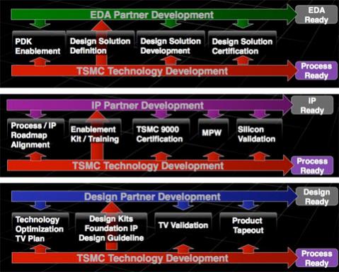
At 65nm TSMC started the OIP program. It began at a relatively small scale but from 65nm to 40nm to 28nm the amount of manpower involved went up by a factor of 7. By 16nm FinFET half of the effort is IP qualification and physical design. OIP actively collaborated with EDA and IP vendors early in the life-cycle of each process to ensure that design flows and critical IP were ready early. In this way, designs would tapeout just in time as the fab was starting to ramp, so that the demand for wafers was well-matched with the supply.
In some ways the industry has gone a full circle, with the foundry and the design ecosystem together operating as a virtual IDM.


Comments
0 Replies to “A Brief History of TSMC OIP”
You must register or log in to view/post comments.