

In 2012 FinFET is one of the most talked about MOS technologies of the year because traditional planar CMOS has slowed down on scaling below the 28nm node. To learn more about FinFET process modeling I attended a Synopsys webinar where Bari Biswas presented for about 42 minutes include a Q&A portion at the end.

Bari Biswas, Synopsys
Bari Biswas is a Sr. Director of R&D for the Implementation Group at Synopsys, responsible for signoff extraction products. He has worked in the area of interconnect modeling, process variation, 3D field-solvers, capacitance and inductance extraction for nearly fifteen years at Avanti and Synopsys. He is the chair for Interconnect Modeling Technical Advisory Board (IMTAB) which defines the direction for interconnect modeling and open source Interconnect Technology Format (ITF). Bari received his MS in Computer Engineering from North Carolina State University at Raleigh and BS in Electrical Engineering from Indian Institute of Technology, Kanpur.
FinFET Overview
What’s wrong with planar CMOS?
- Leakage of planar CMOS devices is too great
- Decreasing mobility (strained silicon helps)
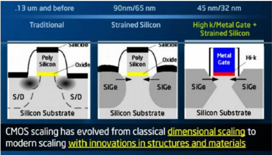
What’s attractive with FinFET?
- Higher performance
- Lower leakage
- Smaller layout area
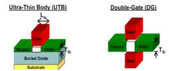
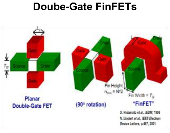
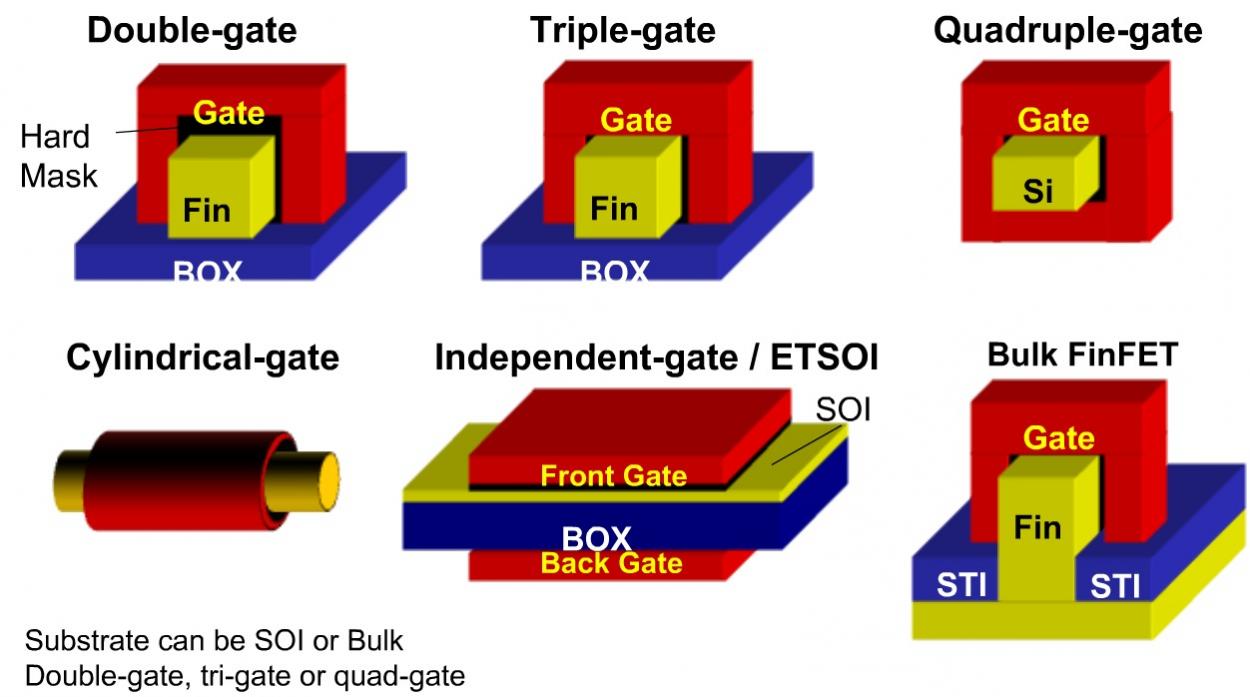
You can have many structures for Multi-Gate:
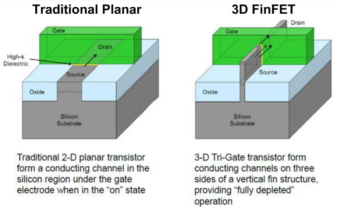
A comparison of a traditional planar MOS device with 3D FinFET:
Intel calls their FinFET a TriGate, and the benefits are:
- Greater drive currents
- Lower switching voltages
- Lower leakage currents
- Lower power, 50%
- Faster switching, 18-37%
- Small wafer cost increase, 2-3% (Source: Mark Bohr, Intel Developer Forum 2011)
Most of the IC layout change is at Metal 1 and lower levels, the higher levels are not impacted with FinFET.
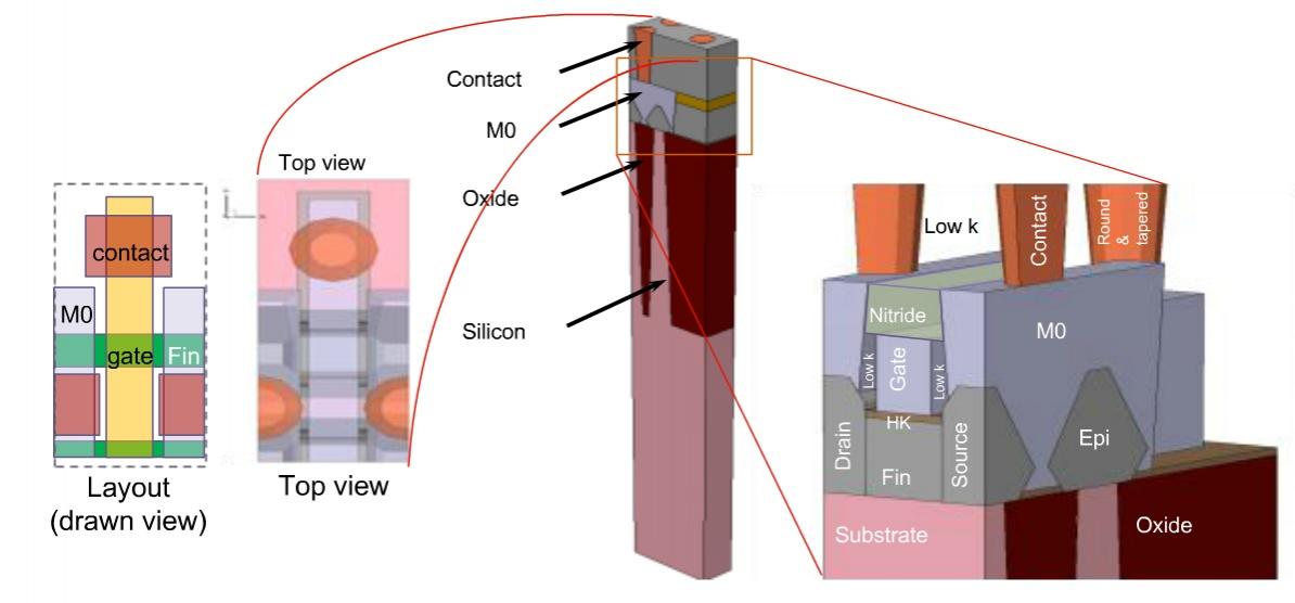
FinFET layout cross-section
Synopsys EDA Tools ready for FinFET
- Sentaurus TCAD, since 2005
- HSPICE using BSIM-CMG models
- StarRC Ultra, since 2008
- IC Validator (DRC, LVS)
- Custom Designer (IC Layout)
- Memory Compilers
- Book co-authored with Chenming Hu (father of FinFET): BSIM4 and MOSFET Modeling for IC Simulation
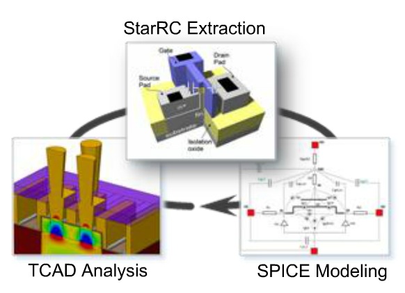
TCAD analysis, extraction and SPICE modeling tool flow work together:
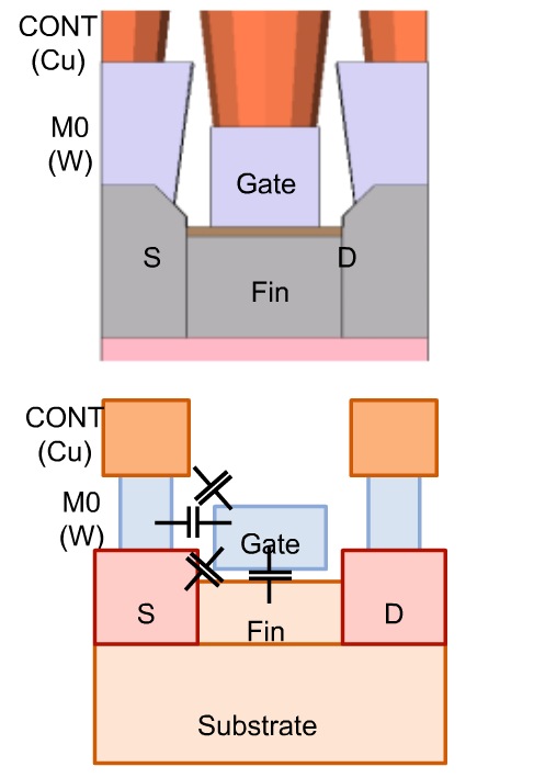
Capacitive coupling has increased between Gate and Source/Drain with FinFET:
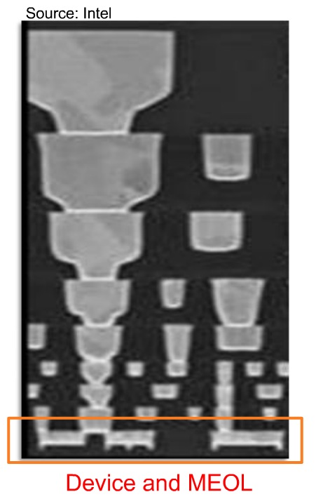
FinFET Mid-end of Line Details
Parasitic modeling becomes critical to get accurate behavior:
Intrinsic capacitances are modeled inside of the SPICE model, while extraction accounts for the remaining capacitances.
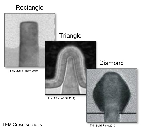
FinFETs can have a variety of shapes based on the foundry preferences, so your TCAD tool captures this layout profile:
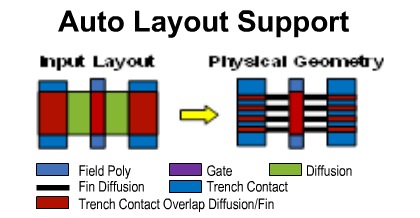
FinFET devices have a quantized effective width based on the height of the device, so multiple fingers are used to create a variety of transistor sizes.
In the Synopsys layout tools you can draw the FinFET width in a simple way, then have it automatically converted into fingers:
A 3D field solver can accurately extract any capacitance value for FinFET layouts however the results are slow, so here’s a comparison between StarRC Ultra(fast extraction) with Rapid3D (most accurate):
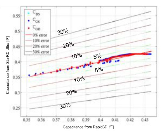
StarRC capacitance results are within +/- 5% of Rapid3D results
Summary
Synopsys has put together an EDA tool flow that handles FinFETS in both an accurate and fast manner for process exploration, cell & macro characterization, and transistor extraction.
Q&A
Q: What’s the reason behind the different FinFET shapes?
A: Each foundry has a different approach to create their FinFET shapes, so we need to model these in our TCAD tool to get accurate parasitics.
Q: How does FDSOI compare to FinFETs?
A: FinFET is also a fully-depleted device for better control. The FDSOI is a continuation of planar CMOS technology, more evolutionary and not so different like FinFET (a disruptive approach).
Q: If FinFETS have so many advantages, where is the foundry support?
A: Intel at 20nm supports FinFET, it’s really up to the foundries to choose when to use this technology.
Q: Is layout always planar, or are FinFETS always laid out?
A: You can layout each Fin or have our tool auto-layout the Fins for you.
Q: Is there any run-time impact for using StarRC Ultra on FinFET?
A: No, not really.
Q: Is there any change to the SPICE simulation flow, or IC layout flows?
A: No, the extraction netlist from StarRC for a FinFET looks like a planar netlist.
Q: Is StarRC currently qualified by foundries for FinFET?
A: Short answer is yes.


Comments
0 Replies to “FinFET Modeling and Extraction at 16-nm”
You must register or log in to view/post comments.