

Last week I reviewed Chapter 1 in the new book: Mixed-Signal Methodology Guide, and today I finish up my review of Chapters 2 through 11. You can read the entire book chapter by chapter, or just jump directly to the chapters most related to your design role or project needs. With multiple authors I was impressed with the wide range of AMS topics they were able to cover from theory to practice. The last sentence in this blog contains a free offer.
Chapter 2: Overview of Mixed-signal Design Methodologies
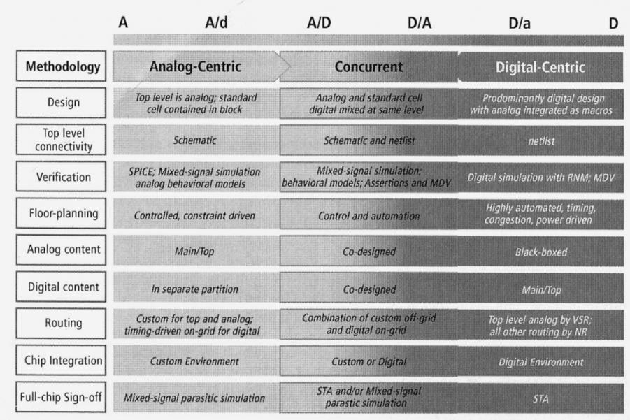
The AMS methodology you choose really depends on what you are designing, so there is no single flow that fits all design styles. Approaches can be top-down, bottom-up, or meet in the middle. There’s a continuum of AMS designs from Analog-centric to Digital-centric.
Historically there were two sets of EDA tools and databases for AMS design: Analog, and Digital. Today however there are common databases and tools for IC design that allow concurrent AMS design.
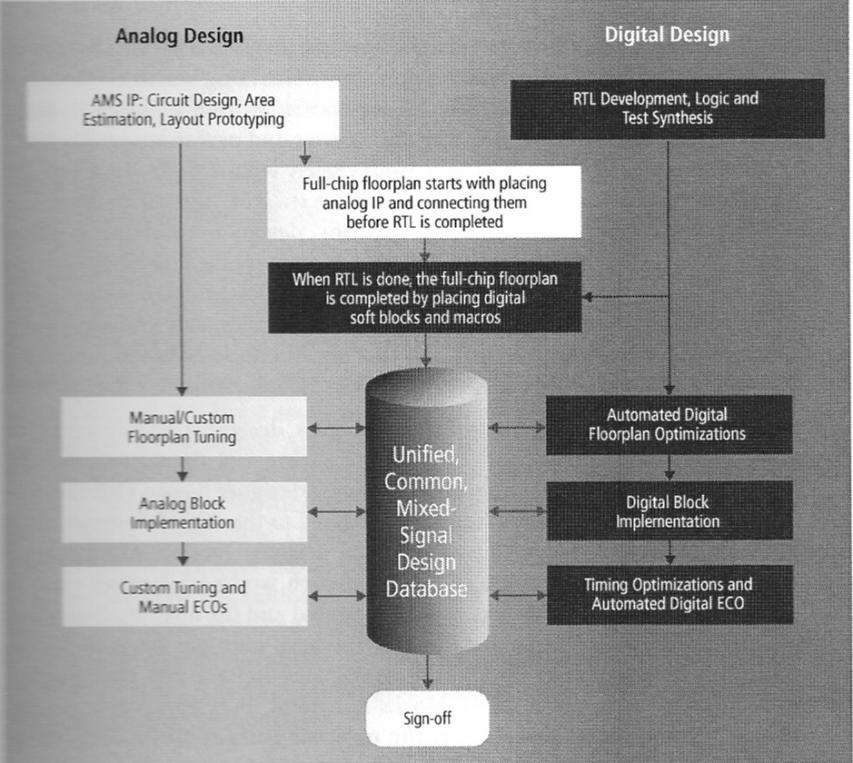
Based on the amount of Analog or Digital in your design you can choose the appropriate design methodology:
Chapter 3: AMS Behavioral Modeling
SPICE circuit simulation can be used on any transistor-level netlist to predict the analog behavior of blocks of your design however at the expense of long run times. If you were to write a behavioral model of your analog block then it could simulate orders of magnitude faster than SPICE. This chapter has plenty of examples on how to start writing AMS behavioral models:
- Programmable Gain Amplifier (Verilog-AMS)
- Analog PGA (Verilog-A)
- Real PGA Model
- Digital PGA Model
- Operational Amplifier (Verilog-A)
- Digital to Analog Converter (Verilog-AMS)
- Low-pass filter (Verilog-AMS)
The concept of Real Number Modeling (RNM) is introduced as a method for analog voltages to be represented as a time-varying sequence of real values.
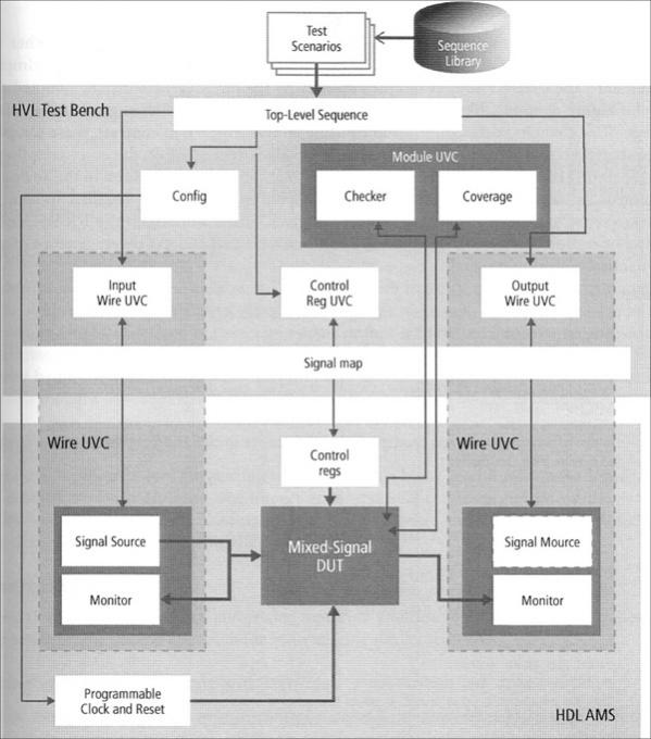
Chapter 4: Mixed-Signal Verification Methodology
At 72 pages this is the longest chapter in the book and reflects that verification consumes more development time and engineering effort than does AMS design, just like in Digital designs. Simulation is the primary tool used to verify an AMS design, unlike in digital where you also have formal methods and Static Timing Analysis.
Assertions are being used in AMS tool flows to capture design intent and report violations. The UVM-MS (Universal Verification Methodology – Mixed Signal) approach offers a direction for a metric-driven verification. Examples of using PSL (Property Specification Language) with Verilog-AMS show how analog events for assertion clocking can be coded.
SystemVerilog Assertions (SVA) are also demonstrated by a mixed-signal Sigma Delta ADC example. Mixed-signal coverage is defined along with mixed-signal metric-driven verification, so engineers can start to measure the effectiveness of their AMS verification.
The Common Power Format (CPF) syntax is used to show how power domains are modeled and the challenges of designing for low power in mixed-signal chips.
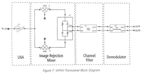
Chapter 5: A Practical Methodology for Verifying RF Chips
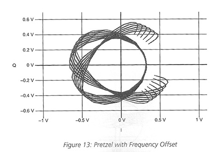
Jess Chen from Qualcomm wrote a math-filled chapter showing how to verify a direct conversion wireless OFDM link. His SystemVerilog code implements a low noise passband amplifier, IQ modulator, IQ demodulator and baseband amplifier.
Simulation waveforms called Pretzels show the behavior of the RF models:
Chapter 6: Event-Driven Time-Domain Behavioral Modeling of Phase-Locked Loops
Verilog-A and Verilog-AMS was used to model a PLL circuit by decomposing the design into several blocks:
- Phase Detector
- Charge Pump
- Loop Filter
- Voltage-Controlled Oscillator
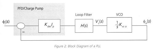
Refinements are shown that add jitter and frequency slewing for a PLL. The benefit of the behavioral model is that you can simulate PLL lock time in seconds instead of using SPICE and having to wait up to a week for results.
Chapter 7: Verifying Digitally-Assisted Analog Designs
The concept of using digital circuits to tune an analog block is gaining use, and Art Schaldenbrand from Cadence provides several examples with calibration to show a new verification methodology:
- VCO with calibration
- Multi-Bit Delta-Sigma ADS with dynamic element matching
- Active-RC filter
Chapter 8: Mixed Signal Physical Implementation Methodology
Two IC layout flows are highlighted: Custom Design, and Constraint-driven.
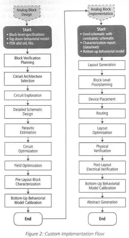
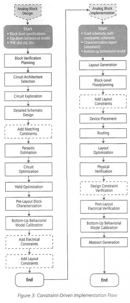
The constraint-driven flow uses Pcells (or Pycells if you prefer non-Cadence tools) to introduce more automation and allow for process migration of analog blocks. The idea is to quickly get from schematic to layout, then use the parasitics from layout back in simulation where performance can be measured and then transistors either re-sized or layout changed.
Physical verification is also touched on:
- LVS (Layout versus schematic)
- DRC (Design Rule Checking)
- ERC (Electrical Rule Checking)
- DFM (Design For Manufacturing)
Chapter 9: Electrically-Aware Design Methodologies for Advanced Process Nodes
Layout Dependent Effects (LDE) can dominate the performance of an AMS design at 28nm and lower process nodes, so using an electrically-aware design methodology can reduce iterations and minimize design time.
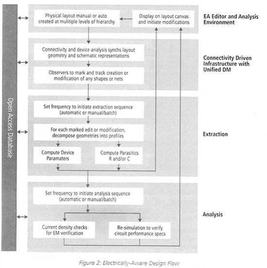
During IC layout the EAD flow will take into account several LDE effects that impact variability and performance:
- Shallow Trench Isolation (STI)
- Well Proximity Effects (WPE)
- Length of Diffusion (LOD)
Reliability concerns like Electromigration (EM) can be analyzed while doing IC layout, instead of waiting for final block assembly.
Chapter 10: IC Package Co-Design for Mixed Signal System
Taranjit Kukal of Cadence wrote about System in Package (SiP) as a way to integrate multiple dies with discrete components into a single package. Our smart phones are probably the most successful example of SiP technology in use today. Multiple ways of implementing SiP were shown:
- Single die in package
- Multi Chip Module (MCM)
- RF module
- 2.5D IC
- 3D IC
- 3D Package
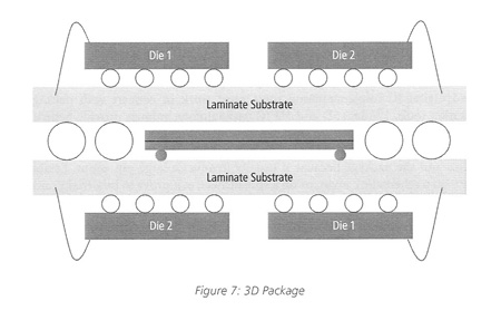
Co-design between package and SiP allows for trade-off analysis early in the system design process, optimized I/O locations, and Power Delivery Network (PDN) analysis.
Chapter 11: Data Management for Mixed-Signal Designs
Michael Henrie and Srinath Anantharaman from ClioSoft described how Design Management (DM) of ICs is different than Software Configuration Management (SCM) because of the broad spectrum of design data:
- Specifications
- HDL design files
- Verification test benches
- Timing and power analysis
- Synthesis constraints
- Place & Route
- Parasitic Extraction
- Standard Cells
- Analog Design
- PDK (Process Design Kits)
- Custom Layout
- GDS II
- Packaging
- Scripts & Customizations
An AMS design management system should enable:
- Collaboration across team members
- Version control
- Release management
- Variant development
- Security and access control
- Audit trail of changes
- Integration with bug tracking
- Design flow integration
- Checkin / Checkout to control access to cells, blocks and modules
- Quick response, low disk space use
- Composite design objects
- Shared workspaces
- Visual change analysis
- Hierarchical design
- Reuse of PDKs
ClioSoft offers one of a few DM tools that work within the Cadence environment and operates on the concept of a repository:
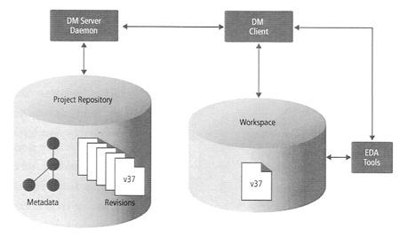
A DM methodology can enable an AMS team to collaborate efficiently, avoid mistakes of data loss, automate version control, analysis changes visually, plus use IP and PDKs across the organization.
Summary
Even if you are a specialist in AMS design and verification you will benefit from the big picture presented in this new book: Mixed-Signal Methodology Guide. The eleven chapters cover a wide range of relevant topics, plus there are ample references to allow you to further explore a topic. I enjoyed the numerous examples provided and code snippets as a way to learn.
As a reward for those who read this blog to the very end I am offering a free copy of the book to the first two people who post a comment and request their copy.


Comments
12 Replies to “Mixed-Signal Methodology Guide”
You must register or log in to view/post comments.