

Collaboration between EDA, Foundry and Design was the key idea today in a webinar hosted by IBM and Cadence about 20nm custom IC design. The three presenters were:

John Stabenow, Cadence
Jeremiah Cessna, Cadence
Keith Barkley, IBM
I blogged about Cadence and John Stabenow back in March and we both live in beautiful Oregon.
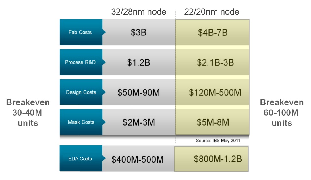
IC design at the 28nm node is expensive and 20nm is even more expensive for foundries and design companies where the break even point is near 100 million units:
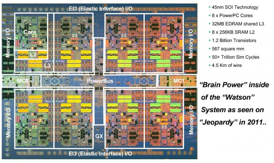
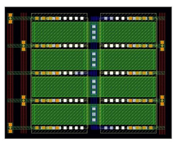
Keith at IBM supports the processor design group, where they designed the CPU that became Jeopardy world champion:
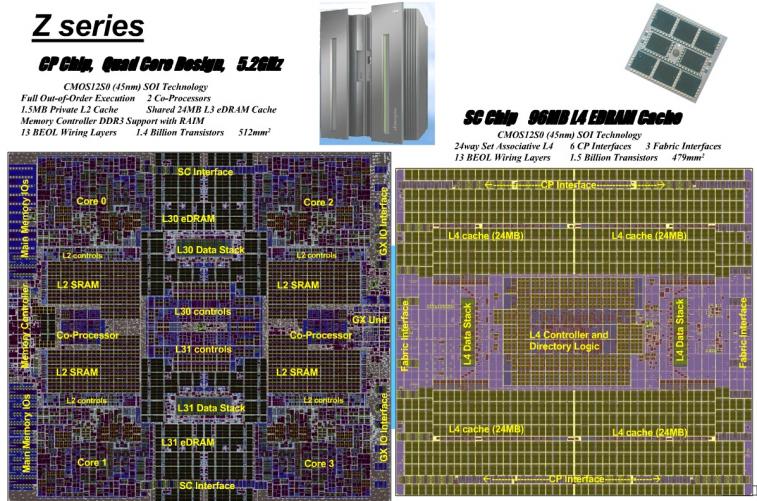
Two more of their billion+ transistor designs:
What IC designers at IBM really want in their design flow:
- Correct by Construction design
- Design Rule and Color Aware (For Double Patterning Technology)
- Must have “base” capabilities with “flexibility”
- Complete “integrated” solution
- Must support “Complex Hierarchical” design flows
- Automatic and “Assisted” interactive capabilities
- etc.
The collaboration between Cadence and IBM have produced EDA tool features like:
- DRD color aware editing
- local interconnect support
- PVS Design rule and color rule checking with fix hints
- PVS decomposition and color balancing
- Correct by Construction design flows
- and more
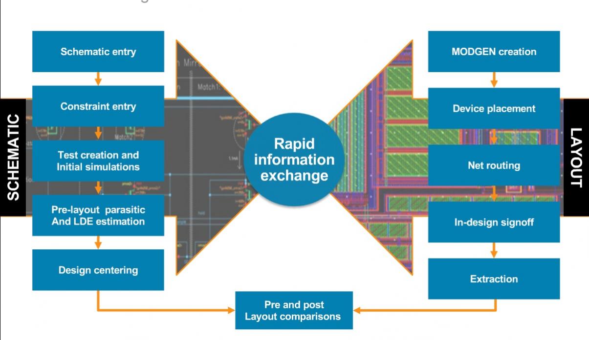
The big picture EDA tool flow from Cadence has both front-end and back-end tools talking to each other, early and often:
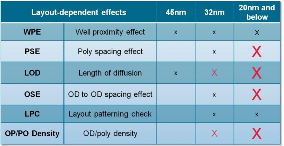
There are six types of Layout Dependent Effects (LDE) that an IC design team needs to be aware of, layout quickly and simulate:
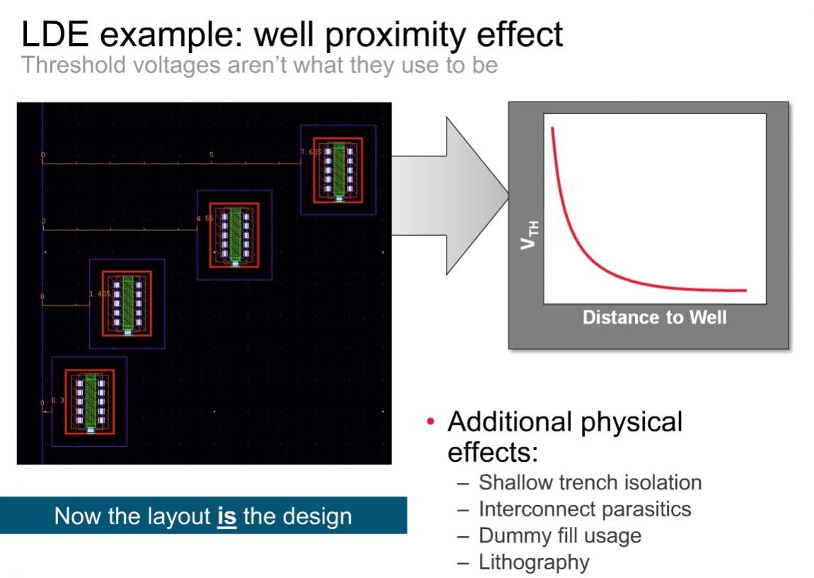
An example of LDE is Well Proximity Effect where the closer you place a transistor to a Well the higher the Vt value becomes which impacts timing and leakage:
One method to get quick feedback on LDE effects is to use automated layout generators instead of manual layout:
Cadence recommends three stages in dealing with LDE effects:
[LIST=1]
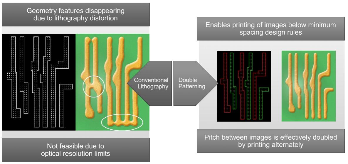
The buzz-phrase for 20nm design in 2012 is “coloring”, which is a technique used in Double Patterning Technology (DPT) where polygons on a single layout layer like Metal 1 are split into two masks (i.e. red and green) in order to actually print the tiny dimensions using the wavelengths of light:
There is some automation available while you interactively use the layout editor Virtuoso to actually see the red and green polygons:
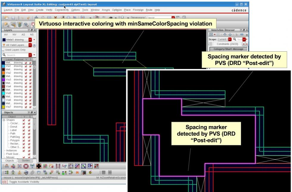
Even when you move cells instances or wire between cells, the Virtuoso tool understands how your critical layers should be automatically decomposed into red and green, or “colored” for use in DPT.
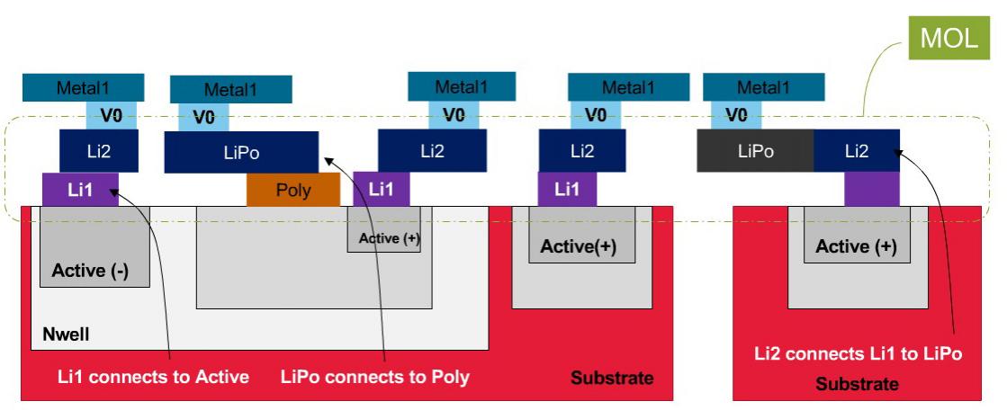
Something new with the 20nm technology at IBM is “local interconnect” which are metal layers that connect by shape overlap without need of a cut layer:
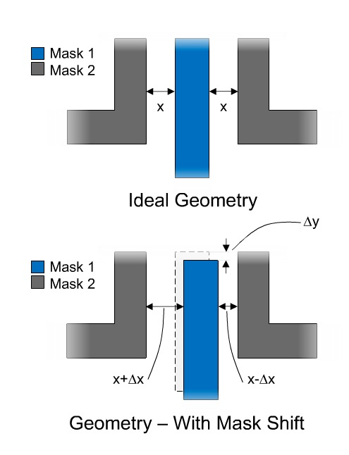
As these DPT masks get shifted then it impacts your layout and the extraction tools need to understand variability and created netlists that let you simulate the effect:
Jeremiah Cessna of Cadence showed some interactive IC layout editing where the coloring in Virtuoso helped you to be compliant with DPT rules.
Summary
I’ve worked at both an IDM (Intel) and EDA companies, so I know how critical it is for collaboration between Foundry, EDA and Design. The folks at Cadence and IBM have been collaborating together and they have the flow and know-how to make 20nm IC design happen for the billion transistor era.
Cadence has some patents in this area of automating “colorizing” and I can understand how they want to protect their intellectual property, so hopefully Mentor and Synopsys can also innovate without violating patents, creating lawsuits, and making the lawyers rich.
Now, it’s up to your finance department to figure out the economic viability of using 20nm versus 28nm or even 45nm (like my new iPad uses) in your next SOC project.
Share this post via:


Comments
5 Replies to “20nm IC Design at IBM using Cadence Tools”
You must register or log in to view/post comments.