

In my last article I talked about the physical design aspect of 3D-IC. Now looking at its verification aspect, it spans through a wide spectrum of test at hardware as well as software level. The verification challenge goes much beyond that of a SoC which is at a single plane. Even a typical SoC that comprises of a processor core, memory controller, GPU, IP block and peripheral units is very difficult to test as a whole system together. A cycle accurate level of testing needs RTL level of description of the whole system and that cannot be attempted at the very early stages of the SoC. Therefore the usual practice is to test the SoC through Virtual Platform to start with. Hardware, software co-verification can take place in the Virtual Platform environment. At this stage, by using SystemC TLM (Transaction Level Modelling), embedded software can be verified at Untimed (UT) and architectural exploration and verification can be done at Loosely Timed (LT) or Approximately Timed (AT) abstraction levels as per need. Most of the major architecture level design issues need be sorted out at this stage. Then the design passes through verification at each stage of design cycle till GDS. Nevertheless, provision for test access architecture like Built-In-Self-Test (BIST) needs to be provided in the chip for testing of manufacturing defects.
Now if we consider a 3D-IC, it can have multiple processor cores, memory controller, cache, high speed peripherals etc. on multiple planes. Each die and the whole stack need to be tested. The dies can come with different IPs or design components from different vendors and can be heterogeneous. The order of magnitude of testing increases exponentially. One faulty die would mean the whole stack to be useless. The individual die can be assumed to be tested by the vendor, provided that is certified on a common test standard. Here are some of the complexities and methodologies of testing which need attention –
Testing in Virtual Platform – Virtual Platform is very appropriate to test the whole system together at higher level of abstraction above RTL. For 3D-IC level of test, it needs to augment the notion of design assembly in multiple planes. The software needs to account for effects of TSVs (Through Silicon VIA) and interconnects across the dies adding into delays.
Die testing – It is important that each die is tested thoroughly to be converted into KGD (Known Good Die). Testability needs to be included by the vendor and that needs test standards, discussed below. Comprehensive testing of die needs more advanced fault models other than stuck-at, bridging and transition faults. Mentor has developed what is called user defined fault model (UDFM) which can be cell aware. The die should also be accessible and testable after being packaged into the stack.
Interposer and TSV testing – Like KGD, interposer and TSV also need to be certified to be known good interposer and TSV for robust inter-die connection and good yield. The die interconnect should be accessible and testable.
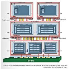
Package (Stack) testing– This needs a test architecture which can enable transport of test data and control signals through all dies and interconnects in the stack. External IOs are typically located at the bottom most die, hence the test signals at a die need to pass through the die below it to finally arrive at the external IO. This asks for a standard configuration of test circuitry at every die which is interoperable as the dies in a stack can come from different vendors. In the stack, testing can be done at partial as well as full stack level.
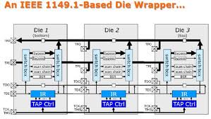
IEEE standards for test – IEEE1149 describes the boundary scan test which is a mature DFT technique used at board level and can be used through the bottom die. IEEE1500 has been developed for test re-use and embedded core test. It has serial as well as parallel test access architecture and rich instruction set for testing cores and associated circuitry. It uses core test language (CTL) for describing test data and wrappers. IEEE1687 describes standard for access and control of instruments embedded into the chip for debugging purposes. To address the issues of heterogeneous dies from multiple vendors, IEEE1838 has been proposed which is die-centric and leverages features from IEEE1149, IEEE1500 and IEEE1687.
Standardizing test access architecture helps IP, die and stack providers to document and deliver appropriate level of information on test access architecture and data. EDA vendors can provide tools to generate and make use of the standard test access architecture. This is specifically necessary for 3D-IC and SoC as there are multiple parties involved in its making.
By Pawan Kumar Fangaria
EDA/Semiconductor professional and Business consultant
Email:Pawan_fangaria@yahoo.com


Comments
0 Replies to “3D-IC Testing – A 3D perspective to SoC”
You must register or log in to view/post comments.