
David Abercrombie from Mentor Graphics met with me on Tuesday at DAC to provide an update on DPT – Double Patterning Technology, something new required for several layers starting at the 20nm node in order to get any IC yield. DPT is also part of Multiple-Patterning.

Source: University of Texas at Austin

David and co-workers have written many detailed blogs about DPT and the effects it has on IC design:
[TABLE] style=”width: 911px”
|-
| valign=”middle” | Title / Link / Author
|-
| valign=”middle” | Double Patterning Requires a Double Take
Semi.Mfg&Design March 2011
David Abercrombie
|-
| valign=”middle” | Double Patterning: Sharing the Benefit and the Burden
Semi.Mfg&Design June 2011
David Abercrombie
|-
| valign=”middle” | Debugging Double Patterning without Getting Double Vision
Semi.Mfg&Design July 2011
David Abercrombie
|-
| valign=”middle” | Multi-Patterning: Game Changer or Y2K?
Semi.Mfg&Design July 2011
Joseph Davis
|-
| valign=”middle” | Gearing Up for a Multi-Patterning World
Chip Design Sept 2011
David Abercrombie
|-
| valign=”middle” | Double patterning from design enablement to verification
BACUS Sept 2011
David Abercrombie
|-
| valign=”middle” | Does Double Patterning Mean The End Of The World?
Electronic Design Nov 2011
Michael White
|-
| valign=”middle” | To Cut or Not To Cut? That is the DP Question
Semi.Mfg&Design Dec 2011
David Abercrombie
|-
| valign=”middle” | While 28 nm Is Still Teething, 20 nm Will Be A Barrel-o-Monkeys
Electronic Design Dec 2011
Michael White
|-
| valign=”middle” | Colorblind—Colorless versus Two-Color Double Patterning Design
Semi.Mfg&Design Mar 2012
David Abercrombie
|-
| valign=”middle” | Double patterning without tears
Tech Design Forum April 2012
Michael White
|-
| valign=”middle” | Anchors Away – Anchoring and Seeding in Double Pattern Design
Semi.Mfg&Design May 2012
David Abercrombie
|-
| valign=”middle” | Interconnect modeling at 20nm – more of the same or completely different?
EE Times May 2012
Carey Robertson
|-
Do I have to use DPT?
For DFM you need to be aware of double patterning technology.
Single patterning with every DFM trick at 20nm you cannot print anything useful.
EUV could be useful however it’s not ready, slow throughput, capacity, costs too high.
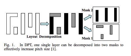
With DPT then 20nm becomes viable again. With DPT there’s enough distance between shapes that a 193nm light source can be resolved.
ebeam is used to create a mask however it takes one day of time, so the throughput is always an issue for Silicon.
OPC was the technology to allow a 193nm stepper to perform at all since 90nm node.
DPT is different however it is used early in the design process.
How to approach DPT:
1) Full Decomposition – designer draws two M1 layers, manually with rules for colored layers. Too much manual work.
2) Colorless – draw one layer, then a special checker will flag what cannot be decomposed and coloring is done before mask prep.
3) Partial decomposition – some auto decompose by designer or the fab. The auto decompose step is creating data, not just checking data.
Challenges to show the designer an odd cycle violation for DPT, show a box region and you need to break the cycle in any one of the spaces. Involve the IC designer in how to fix each DPT violation.
TSMC says no to stitching, keep life simple.
Common Platform Alliance – yes, we accept stitching.
Patented approach – where is DPT not possible because of odd-cycle coloring issues? Red is conflict, orange area is a warning. Much more visual feedback on how to fix this.
Demo – In SpringSoft Laker a layout was run through a color check, then it highlighted in Orange and Red colors. Use Calibre RealTIme to help identify what cannot be colored.
Which layers: Rx (Active), Contact, M1, via 2 – 6.
Virtuoso customers want RealTime to work in their environment however Cadence would need to agree, because they compete with RealTIme and have an equivalent tool (but no warning rings like Calibre).
Calibre Multi-patterning – is the tool that does the decomposition, stiching or not, with or without warning rings, decomp or colorless flows.
P&R can use cells that are over-designed. Olympus is coloring aware.
Calibre plus Encounter (Cadence) or Synopsys also works, ATop Tech. Pyxis.


Comments
6 Replies to “Double Patterning Technology at DAC”
You must register or log in to view/post comments.