
It’s no coincidence that the TSMC Symposium is right after the Q1 earnings call. This will allow TSMC to talk more freely and they certainly will, my opinion. It is a very interesting time in the semiconductor industry and TSMC, being the bellwether, can tell us what will happen the rest of the year and give us some 2020 insights.
TSMC CEO C.C. Wei again led the call with a prepared statement. This time I will paste the entire statement (minus the packaging stuff) with my embedded comments.
- Thank you, Lora. Good afternoon, ladies and gentlemen. Let me start with our near-term demand and inventory. We concluded our first quarter with revenue of TWD 280.7 billion or USD 7.1 billion, in line with our revised guidance. Our business in the first quarter was impacted by three factors: first, the overall global economic condition, which dampened the end market demand; second, customers are ongoing inventory adjustment; and third, the high-end mobile product seasonality. Meanwhile, the net effect from the photoresist defect material incident also impact our first quarter revenue by about 3.5%.
My question here is: Who is liable for this defect? Is the supplier being held accountable? Accounts of this incident from South Korea painted TSMC as negligent which I have found to be fake news.
- Moving into second quarter this year. While the economical factor and mobile product seasonality still linger, we believe we may have passed the pattern of the cycle of our business as we are seeing customers’ demand stabilizing. Based upon customer indications for their business and wafer loading in second quarter, we also expect our customers’ overall inventory to be substantially reduced and approach the seasonal level around the middle of this year.
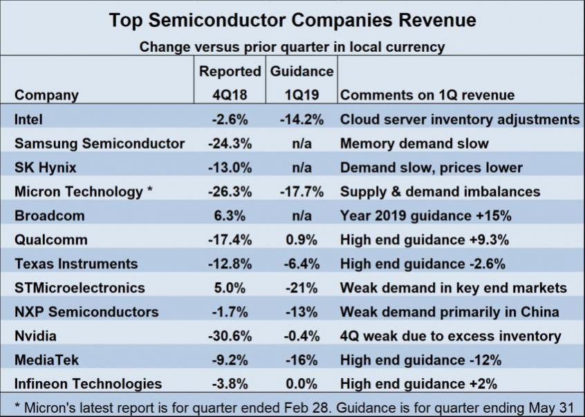
Personally, I feel the second quarter will be stronger than expected based on 2018 year end CEO comments. It is better to under predict than over predict and I believe that is what is happening here. Let’s not forget the Q1 2019 semiconductor guidance we previously published:
- In the second half of this year, TSMC’s business will be supported by this year’s inventory base as well as strong demand from our industry-leading 7-nanometer technology, which support high-end smartphone new product launches, initial 5G deployment and HPC-related applications. For the whole year of 2019, we forecast the overall semiconductor market is good in memory as well as foundry growth to both be flattish. For TSMC, we reiterate that we expect to grow slightly in 2019.
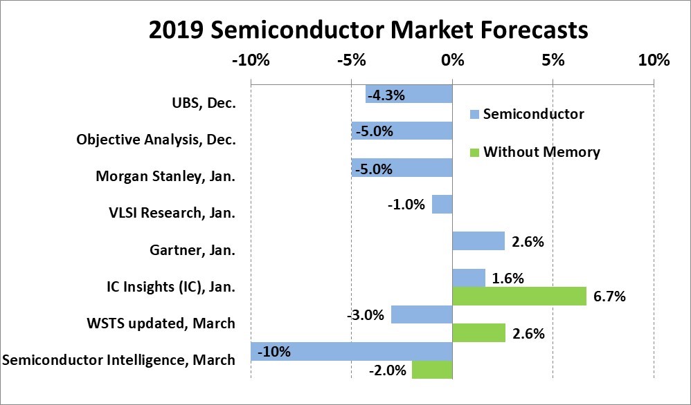
To me this is low single digits but closer to 5% than 1%. Here are the previously published analyst forecasts for 2019:
- Now let me update the photoresist material incident. On February 15, in order to ensure quality of wafer delivery, TSMC announced it will scrap a large number of wafers as a result of a batch of bad photoresist material from a chemical supplier. This batch of photoresist contain a foreign polymer that created a desirable – undesirable effect and resulted in yield deviation on 12-and 16-nanometer wafers at Fab 14B.
- We have since taken corrective action to enhance our defenses and minimize future risk. Our actions including the following: improved TSMC’s own in-house incoming material, conforming test and controls; upgrade control and methodology with all suppliers for incoming material quality certification; establish robust in-line and off-line monitoring process to prevent defect escape.
TSMC does not point fingers but again I would like to know more about this event.
- Now I will talk about our N5 status. Our N5 technology development is well on track. N5 has entered risk production in first quarter, and we expect customer tape-outs starting this quarter and volume production ramp in first half of 2020. With 1.8 times logic density and 15% speed gain and an ARM A72 core compared with 7-nanometer, we believe our N5 technology is the most competitive in the industry. With the best density performance, power and the best transistor technology, we expect most of our customers who are using 7-nanometer today will adopt 5-nanometer. With N5, we are expanding our customer product portfolio and increasing our addressable market. Thus, we are confident that 5-nanometer will also be a large and long-lasting node for TSMC.
To be clear TSMC 5nm chips will be in Apple products next year. I have read reports that TSMC released 6nm because 5nm was late which is fake news. I know many companies that are taping-out at 5nm and it is on track and meeting expectations. More details will be available on SemiWiki after the symposium so stay tuned.
- Now I’ll talk about the ramp up of N7 and N7+ and introduction of N6. We are seeing strong tape-out activity at N7, which include HPC, IoT and automotive. Meanwhile, our N7+, which adopts EUV for few critical areas, has already started volume production now. The yield rate is comparable to N7. We’ll reaffirm N7 and N7+ will contribute more than 25% of our wafer revenue in year 2019.
If you look at TSMC’s Q4 2018 revenue split, 50% is FinFET processes and 50% is mature CMOS nodes. In Q4 2017 FinFET processes were 45% and in Q4 2016 it was 33%. In Q1 2019 FinFET revenue dropped to 42%, not a good sign, let’s blame cryptocurrency.
- As we continue to improve our 7-nanometer technology and by leveraging the EUV landing form, N7+, we now introduce N6 process. N6 has three major advantage. First, N6 have 100% compatible design rules with N7, which allows customer to directly migrate from N7-based design, which substantially shorten the time-to-market. Second, N6 can deliver 18% higher logical density as compared to N7 and provide customer with a highly competitive performance-to-cost advantage. Third, N6 will offer shortened cycle time and better defect density. Risk production of N6 is scheduled to begin in first quarter year 2020 with volume production starting before the end of 2020.
N6 is a little bit confusing thus far. Hopefully we can get it cleared up at the TSMC Symposium. From what I understand N7 and N7+ are not design rule compatible since N7+ has EUV. N6 is N7+ with an additional layer of EUV which helps with density. Saying N6 and N7+ are design rule compatible makes sense but is N6 really design rule compatible with N7?
- Finally, I will talk about the HPC as our most important growth driver in the next five years. CPU, AI accelerator and networking will be the main growth area for our HPC platform. With the successful ramp of N7, N7+ and the upcoming N6 and N5, we are able to expand our customer product portfolio and increase our addressable market to support applications, such as data center, PC and tablets. Meanwhile, we also see networking querying thanks to 5G infrastructure deployment over the next few years. We are truly excited about our growth opportunities in HPC. Thank you for your attention.
AI is a trending term on SemiWiki and readership is all over the map. I seriously doubt it will be a quick bubble like cryptocurrency or even a 10 year bubble like mobile. In my opinion AI will be with us for a very long time and it will consume leading edge wafers like a zombie apocalypse, absolutely.
From what I have heard EUV throughput is still ramping up so my fingers are crossed for 5nm. Hopefully EUV is covered in more detail next week at the TSMC Symposium. I will also get a refresh from our resident EUV expert Scott Jones. In fact, he has just posted an EUV blog from SPIE:
SPIE Advanced Lithography Conference – Imec and Veeco on EUV
Bottom line: The second half of 2019 will be good for TSMC and 2020 will be even better. My prediction today for TSMC in 2020 is back to double digit growth. Remember, now that Intel is out of 5G modems TSMC will get the modem business back from Apple next year via the 7nm QCOM modem plus other 5G modem business. 2020 will be the beginning of a beautiful 5G friendship.
Share this post via:


Comments
18 Replies to “TSMC Q1 2019 Earnings Call Discussion!”
You must register or log in to view/post comments.