
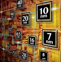
 Last week TSMC announced the availability of its complete 5nm design infrastructure that enables SoC designers to implement advanced mobile and high-performance computing applications for the emerging 5G and AI driven markets. This fifth generation 3D FinFET design infrastructure includes technology files, PDKs (Process Design Kits), tools, flows and IPs –all of which have been developed and validated by multiples silicon test vehicles through earlier collaboration with leading EDA and IP vendors.
Normally each process node shift is expected to deliver significant improvements in one or more of PPAC (Performance, Power, Area or Cost) design metrics. For example, the innovative scaling features in full-fledged EUV 5nm node provides a 1.8X logic density and 15% speed gain based on the ARM® Cortex®-A72 core testcase. While the process refresh update seems so regular (about every 18 to 24 months), the intricacies imposed by the new process technology keep rising and its direct impacts on the EDA space have been constantly endured foremost by both the physical verification and circuit simulation tools.
 Mentor, a Siemens Business has been the industry leader in providing physical verification solution through its Calibre physical verification (PV) platform, which includes Calibre nmDRCand Calibre nmLVS. As a design signoff tool, there are three most sought criteria in PV: accuracy, reliability and performance –all of which are attainable through tight collaboration with both the targeted foundry and alpha customers. Foundry rigorous trials such as TSMC applied double-blind QA procedure has helped to facilitate tool and design flow readiness.
Design Density, Performance and Rule Complexity
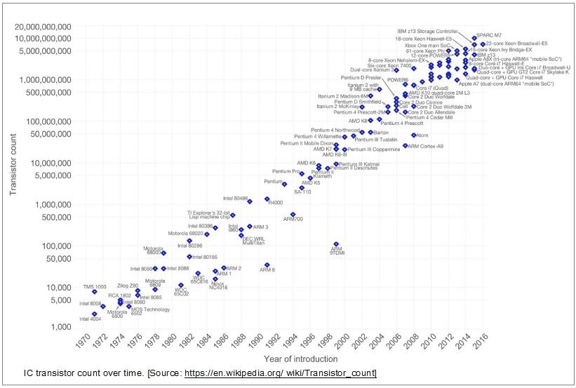
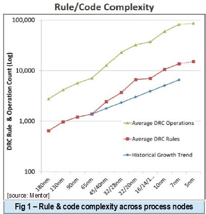 As physical verification has evolved around design rules development and its verification, the rule complexity is directly proportional to the device and interconnect technology of the underlying process. Despite the slow down of Moore’s law, design density is still increasing driven by the relentless compute power demand to process data on the cloud and edge. Historically, transistor count has been used as the classic metric to measure the forward trend. Recent multi-core design and increased IPs inclusion trends have driven the transistor counts, pushing the number of design rules and the associated operations needed to implement those rules upward. The non-linear growth of DRC rules prompts challenges to a timely adoption of new process shift by the design teams.
Deep Collaboration and EDA Tool Certifications
A key success criterion for tool certification is to incorporate new functionality based on the foundry requirements in the early stages of process node development. During this development stage, foundry needs to step through the learning curve and bootstrap their prior known node experiences to enhance the overall ramp time. Over the years, Mentor has participated in repeat successful collaboration including three main physical verification areas (DRC, LVS, xACT/xRC) with multiple foundries.
To have foundries utilize Calibre tools internally as they develop a new process provides the most valuable return as it allows earlier identification and simultaneous fine-tuning of foundry design requirements and hardening the verification tools with any needed rules. For example, Mentor Calibre has been part of the TSMC EDA tool certification.
“TSMC’s 5-nanometer technology offers our customers the industry’s most advanced logic process to address the exponentially growing demand for computing power driven by AI and 5G,”said Cliff Hou, Vice President of Research & Development/Technology Development at TSMC. “5-nanometer technology requires deeper design-technology co-optimization. Therefore, we collaborate seamlessly with our ecosystem partners to ensure we deliver silicon-validated IP blocks and EDA tools ready for customer use. As always, we are committed to helping customers achieve first-time silicon success and faster time-to-market.”
In very advanced node such as TSMC 5nm, a deeper design-technology co-optimization is also necessary. Such earlier and heuristic collaborative efforts among foundry, EDA provider and the alpha customer will culminate in a number of pilot tapeouts and the start of silicon risk production cycle. For example, the flurry of pilot 5nm tapeouts occurring in the last few quarters will be followed by silicon bring-up in the second half of 2019.
 Tool Capacity, Memory and Runtime
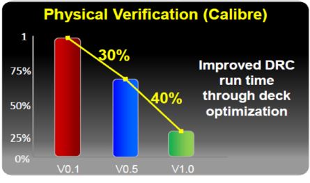
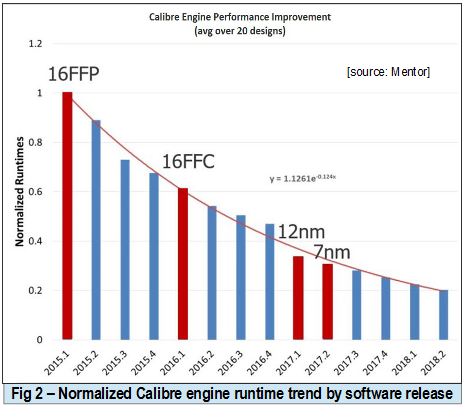
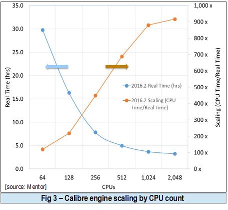
Tool scalability involves several variables such as code vectorization and optimal memory footprint. Memory usage is a key metric that also ties to tool performance. The diagram in figure 2 shows the normalized Calibre engine performance trend as a result of incorporating continuous speed improvements over several process nodes. In two recent Calibre nmDRC versions across six different 7 nm designs, Mentor reported a consistent 40-50% decrease in memory usage as the underlying data structures and memory management techniques were improved.
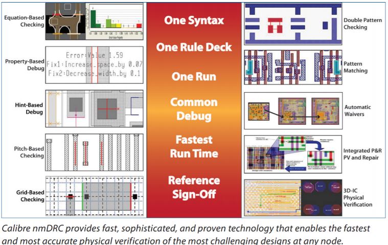
Calibre facilitates pre- and post- physical validations by providing ease-of-use interfaces for navigating and visualizing complex verification errors. Without proper integration and planning, completing a verification task may incur significant post-run analysis time. This can be minimized by enabling the many available Calibre features to configure, launch, review, and debug within the designer’s chosen flow as it is built to accommodate many third party and design team internal flows. For example, Calibre has uniquely used special debug layers for double-patterning debugging, and automated waiver processing for masking out IP errors during chip integration debugging.
The immense challenges of a process node shift have strained silicon ecosystem stakeholders which include foundries, designers and EDA companies. Aside from having ample solution expertise and commitment, EDA company such as Mentor has resorted in deep collaboration and partnership with foundries and designers to perform early process exploration and enabling successful deployment of the needed toolset including Calibre physical verification tools.
Check HERE for more discussion on Mentor Calibre physical verification tool for advanced process node.
Share this post via:


Comments
There are no comments yet.
You must register or log in to view/post comments.