
On April 2 – 4, the 2019 International Conference on Frontiers of Characterization and Metrology for Nanoelectronics (FCMN) will be held at the Monterey Marriott in Monterey, CA. The 2019 FCMN is the 12th in the series that began in 1995 with a keynote talk by Craig Barrett, ex-CEO of Intel.

As its title says, FCMN focuses on all aspects of characterizing and measuring nanoelectronic devices and materials, covering device research, development, and manufacturing. That includes the whole spectrum of techniques: chemical, physical, electrical, magnetic, optical, in-situ, and real-time control and monitoring. As such, there is likely to be a topic of interest to almost anyone engaged in the metrology and analysis of semiconductor products and manufacturing, and beyond.
After the plenary session starting the conference, the breadth of the conference can be seen in the session titles – AI, Machine Learning, and Hybrid Metrology; and Microscopy (Tuesday), Magnetics/Spintronics; Metrology for Patterning; 7-10 nm Metrology and Defect Inspection; Nanoscale and Interfacial Compositional Characterization and Metrology (Wednesday), Metrology for Advanced Packaging; Emerging Characterization and Metrology; “General”; TCAD; and Metrology for Silicon Photonics and Sensors (Thursday). Over the three days, there are 34 presentations, and unlike some conferences, no parallel sessions.
On the Tuesday and Wednesday evenings there are formal poster sessions, but they are also available for viewing in the coffee and lunch breaks through to the Thursday lunchtime; with 46 papers to view, there’s good opportunity to talk with the authors.
Socially, there is the opening reception at 6.30 on Monday 1st April, the conference banquet on Tuesday evening, and drinks and snacks will be served at the evening poster sessions.
Tuesday
After the conference opening, by long-term conference chair David Seiler, we have three keynote talks:
- Beyond CMOS Computing, from Ian Young of Intel
- Frontiers in Memory Technology and Metrology Drivers, by Gurtej Sandhu of Micron
- Impact of Quantum Information Science on the Future of Nanoelectronics, by Carl Williams, NIST
In the first session, AI, Machine Learning, and Hybrid Metrology, which is spread over lunch, we have three papers on deep learning/machine learning/AI, from imec, Oakridge Labs, and Nova Instruments.
- Machine Learning and Deep Learning Opportunities for Metrology and Process Control, Phillip Leray, Imec
- Deep Learning in Atomically Resolved Imaging: from Learning Physics to Atom by Atom Fabrication, Sergei Kalinin, Oakridge
- AI and Machine Learning for Advanced Semiconductor Metrology and Process Control, Shay Wolfling, Nova
Then we get into the Microscopy session, with a variety of techniques:
- What Does Near-line TEM Bring to the Table for the CMOS Manufacturing Industry? Paul van der Heide, imec
- When Ion or Electron Channeling meets Crystal Orientation Mapping, Anne Delobbe, Tescan Orsay
- Low Energy Electron Resist Exposures, Rudolf Tromp, IBM
- Accurate and Precise Analysis of Nanoscale Semiconductor Devices with Atom-probe Tomography: a Physicist’s Dream or an Analyst’s Nightmare? Wilfried Vandervorst, imec
The last paper of the session is a must-see for me, since looking at the current generation of 7-nm going down to 5-nm devices, we are literally counting atoms when we try and analyse them, and the atom probe is the last resort for trying to do chemical analysis of the doping of these parts. I suspect the answer is closer to the nightmare, since there are so many opportunities for contamination and error; but I have known Wilfried for years, and he is an engaging speaker with likely some tantalising information for us.
After the last paper we have posters (I will detail them after going through the spoken presentations), hors d’oeuvres and drinks, followed by the banquet.
Wednesday
First up, we start with Magnetics/Spintronics; MRAM was one of the significant topics at last year’s IEDM conference, so it will be interesting to see the characterization techniques required:
- Metrology for the Manufacturing Needs of MRAM, Daniel Worledge, IBM
- Metrology for Topological Spintronics Materials and Devices, M. Zahid Hasan, Princeton
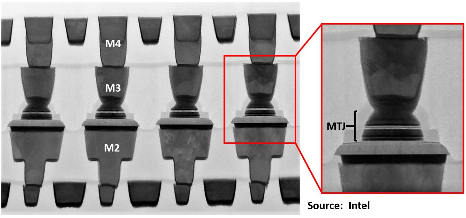
- Three-Dimensional Structural and Compositional Analysis of MTJ by STEM/EDX Tomography, Yuji Otsuka, Toray Research Center
Magnetic tunnel junctions (MTJs) require a complex stack of materials, often nanometer-scale, so even with TEM/STEM capability, the structure is not clear. As an example, this is the MTJ from Intel’s IEDM paper [1]:
After coffee we have Metrology for Patterning, taking us to lunch:
- CD, THK and Emerging Metrology Solutions for 3D Transistors and Multi-step Patterning, Alok Vaid, GLOBALFOUNDRIES
- Interlayer Edge Placement Hotspots: Quantifying and Expanding Combined CD/Overlay Process Window, John Sturtevant, Mentor Graphics
- Optical Critical Dimension Metrology in Memory and Logic, Andy Antonelli, Nanometrics
- Holistic Metrology Approaches for Improved Device Overlay and Edge Placement Error, Arie den Boef, ASML
And after lunch there is 7-10 nm Metrology and Defect Inspection, with one optical and two e-beam papers:
- Advancement on Optical Inspection Technology for 7nm or Below Process Development and Manufacturing, Yalin Xiong, KLA-Tencor
- Extending Electron Beam Technology Further/Deeper into the Metrology Space for 7nm or Below Process Development and Manufacturing, Ofer Adan, AMAT
- Advancement on Massively Parallel Electron Beam Inspection Technology for 7nm or Below Process Development and Manufacturing, Oliver Patterson, HMI
I’m always amazed that optical inspection still works at the nanometer scale, so the first talk will hopefully give me some clues as to how; and even e-beam is challenged by stochastics at these generations, so the AMAT (Applied Materials) and HMI (Hermes Microvision, now part of ASML) presentations will bring me up to date.
To finish the afternoon, we have the Nanoscale and Interfacial Compositional Characterization and Metrology session:
- Micro X-ray Fluorescence for Integrated Dopants and Thin Film Analysis, Wenbing Yun, Sigray
- Integrated Process Learnings with Hybrid Characterization, Ying Zhou, Intel
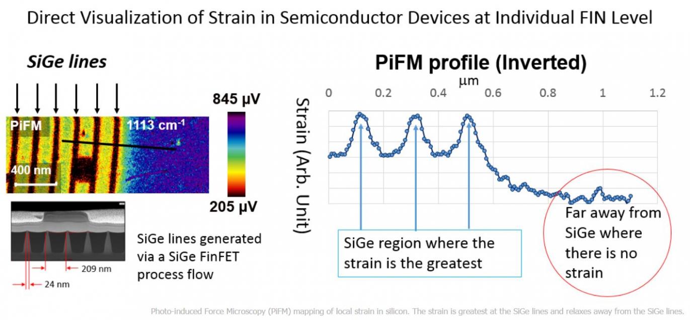
- PIFM Nanoscale Chemical Probe for Novel Patterning Applications, Tom Albrecht, Molecular Vista
I had no idea what PIFM is, so I checked out the Molecular Vista website – it translates to photo-induced force microscopy, another application of the (now) venerable atomic force microscope (AFM). In PIFM, the probe tip detects the force gradient created by interaction between a metal coated AFM tip and optically-driven dipoles in the sample, illuminated by a pulsed laser.
Here’s an example of strain measurement in SiGe fins using PIFM, taken from their website:
Again, we have posters, hors d’oeuvres and drinks from 5.30 – 6.30.
Thursday
There are three talks in the first session, Metrology for Advanced Packaging:
- Existing and Future Characterization Needs, Christian Schmidt, NVIDIA
- Really Nondestructive High-resolution X-ray Tomography for Advanced Packaging Applications, Ehrenfried Zschech, Fraunhofer IKTS Dresden
- Nondestructive and Economical Dimensional Metrology of Deep Structures, Ravikiran Attota, NIST
High-performance products such as NVIDIA’s are taking us into the world of 3D-stacked high-bandwidth memory (HBM) and interposers, which provide metrology and testing challenges of their own, and we are likely to see stacks of direct-bonded chips too; so x-ray tomography and deep-structure metrology are likely quite applicable to future parts such as AI or cloud server devices.
Next up (after coffee) is Emerging Characterization and Metrology:
- Current Status and Future Possibilities of HHG Sources for Characterization/Metrology in the Semiconductor Industry, Brennan Peterson, KMLabs
- Atom Probe Tomography: Toward Improved Productivity and Correlative Analysis in the Semiconductor Industry, David Larson, Ametek
- Current Status and Future Prospects for SPM for Supporting the Semiconductor Industry, Peter De Wolf, Bruker
- Hybrid SIMS: How the Orbitrap Mass Analyzer Can Improve the Self-Focusing SIMS Concept for Advanced Semiconductor Structures, Alexis Franquet, Imec
High-harmonic generation (HHG) from lower-wavelength laser light enables table-top emission of EUV radiation for analysis and imaging; and we’ll see what David Larson has to say, after Wilfried Vandervorst’s talk on Tuesday. Scanning probe microscopy (SPM) has come a long way from the original AFM, so an update on the latest techniques will be useful, and as SIMS is always a challenge in nanoscale analysis, I’m curious about imec’s presentation.
Lunch gives the last chance to check out the posters, then we have three one-paper sessions, General:
- Metrology Requirements for Next Generation of Semiconductor Devices, George Orji, NIST
Then TCAD:
- Electromigration Power Grid Checking – Novel Design and Reliability Metrology, Valeriy Sukharev, Siemens/Mentor Graphics
And Metrology for Silicon Photonics and Sensors:
- Scanning Probe Technology to Make Local, Non-Contact Measurements of Photonic Circuits, Vladimir Aksyuk, NIST
The conference ends on a high note with a keynote from Dan Hutcheson:
- Moore’s Law in a Neuromorphic World, Dan Hutcheson, VLSI Research
The industry is currently shifting from von Neumann to neuromorphic architectures, moving from digital devices to analog cells capable of storing weights in a single device rather than in bytes of bits. Dan will discuss how this will be a disruptive change, since he believes the wafer fab quality standard can no longer be ‘defect free.’ It must be ‘correct by construction.’ That will mean tremendous opportunities for process diagnostics in the world of neuromorphic competition.
Poster Papers
There isn’t space here to look at all 46 poster papers, but to my surprise I want to view at least twenty of them:
- 001, Metrology of Semiconductor Devices Using Machine Learning and Active Shapes, John Flanagan, et al., Thermo Fisher Scientific
- 002, Image-based Dimensional Analysis for Semiconductor and MEMS Structures, Woo Sik Yoo, et al., Wafermasters
- 004, Automatic Data Acquisition and Analytical System for High Quality Metrology, S. Kawai, et al., JEOL
- 006, Influence of Contacted Poly Pitch Dimension on Channel’s Strain Level in 22nm UTBB FDSOI PMOSFET Technology, F. Ravaux et al., Khalifa U., GLOBALFOUNDRIES
- 007, A 331-Beam SEM, C. Riedesel, et al., Carl Zeiss Microscopy GmbH
- 010, Understanding the Role of Scanning Electron Microscope Image Noise in the Measurement of Pattern Roughness, Chris A. Mack, et al., Fractilia, imec
- 015, 3D Metrology by FIB-SEM Tomography, Amir Avishai, et al., Carl Zeiss
- 019, Micro Four-Point Probe Seebeck Measurements on nm-Wide Si Fins, M.-L. Witthøft, et al., Tech. U. Denmark, imec, KU Leuven, CAPRES A/S
- 020, Understanding of and Opportunities for Electrical Characterization of Scaled Devices Using Scanning Spreading Resistance Microscopy, Kristof Paredis, et al., imec, KU Leuven
- 024, Atom Probe Tomography Using Extreme-Ultraviolet Light, Luis Miaja-Avila, et al., NIST, Colorado School of Mines
- 026, Differential Hall Effect Metrology (DHEM) for Depth Profiling of Electrical Properties at High Resolution, Abhijeet Joshi, et al., Active Layer Parametrics (ALP), SUNY Polytechnic Institute
- 027, Size Effects on Dopant Activation in Si Fins, S. Folkersma, et al., imec, KU Leuven, Tech. U. Denmark, CAPRES
- 028, Near-Surface Sub-nm Resolution Activation Profiles in P and Sb+P Doped Ge, Pranav Ramesh, et al., Stanford U, ALP, EAG Laboratories
- 030, Latest Advancements in Nanoscale IR Spectroscopy for Failure Analysis of Electronic Devices, Anirban Roy, et al., Bruker
- 031, High Resolution Secondary Ion Mass Spectroscopy (SIMS) for Characterization, Brett Lewis, et al., Carl Zeiss
- 033, 3D Atomistic Mapping in Group-IV Ultrathin Silicon Germanium Superlattices, Samik Mukherjee, et al., Ecole Polytechnique de Montreal, Applied Materials
- 041, Analysis Lab Will Be placed on in-FAB Metrology? Kyung Woo Lee, et al., Samsung Electronics
- 042, Ions and Chemistry to Fulfill Observation and Probing Specifications of sub-28nm Devices, G. Goupil, Orsay Physics/Tescan Orsay, ST Microelectronics, Infineon Technologies, Fraunhofer Institute IMWS
- 043, Electric Field Gradient Reference Material for Scanning Probe Microscopy, J. J. Kopanski, et al., NIST
- 046, Super-Resolution Single-Molecule Microscopy: a Characterization Tool for Materials, J. Alexander Liddle, et al., NIST, Northwestern U., IREAP
The full schedule, including the posters, isavailable from the FCMN website. I hope to see you there!
Share this post via:


The Data Crisis is Unfolding – Are We Ready?