

3D ICs complicate silicon testing, but solutions exist now to many of the key challenges. – by Stephen Pateras
The next phase of semiconductor designs will see the adoption of 3D IC packages, vertical stacks of multiple bare die connected directly though the silicon. Through-silicon vias (TSV) result in shorter and thinner connections that can be distributed across the die. TSVs reduce package size and power consumption, while increasing performance due to the improved physical characteristics of the very small TSV connections compared to the much larger bond wires used in traditional packaging. But TSVs complicate the test process, and there is no time to waste in finding solutions. Applications involving the stacking of one or more memory die on top of a logic die, for example using the JEDEC Wide IO standard bus interface, are ramping quickly.
One key challenge is how to test the TSV connections between the stacked memory and logic die. There is generally no external access to TSVs, making the use of automatic test equipment difficult if not impossible. Functional test (for example, where an embedded processor is used to apply functional patterns to the memory bus) is possible but is also slow, lacks test coverage, and offes little to no diagnostics. Therefore, ensuring that 3D ICs can be economically produced calls for new test approaches.
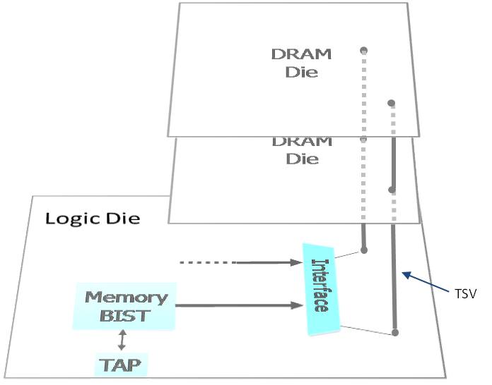
A new embedded test method that works for test and diagnostics of memory on logic TSVs is built on the Built-In Self-Test (BIST) approach that is already commonly used to test embedded memories within SoCs. For 3D test, a BIST engine is integrated into the logic die and communicates to the TSV-based memory bus that connects the logic die to the memory as illustrated in Figure 1.
For this solution to work, two critical advances over existing embedded memory BIST solutions were necessary.
One is an architecture that allows the BIST engine to communicate to a memory bus rather than directly to individual memories. This is necessary partly because multiple memories may be stacked within the 3D IC, but mostly to allow the BIST engine to test the memory bus itself, and hence the TSV connections, rather than just the memories. Test algorithms tailored to cover bus-related failures are used to ensure maximum coverage and minimal test time. Because of this directed testing of the memory bus, the 3D BIST engine can also report the location of failures within the bus, which allows diagnosis of TSV defects.
The second critical advance in this new 3D BIST solution is that it is run-time programmable. Using only the standard IEEE 1149.1 JTAG test interface, the BIST engine can be programmed in silicon for different memory counts, types, and sizes. Because the BIST engine is embedded into the logic die and can’t be physically modified without a design re-spin, this adaptability is essential. With full programmability, no re-design is needed over time even as the logic die is stacked with different memories and memory configurations for different applications.
An automated flow is available for programming the BIST engine (for wafer or final package testing) to apply different memory test algorithms, to use different memory read/write protocols, and to test different memory bus widths and memory address ranges. The patterns needed to program the engine through the JTAG interface pins are generated in common formats, such as WGL or STIL, to be loaded and applied by standard automatic test equipment.
Because this 3D test solution is embedded, it needed to have minimal impact on design flows and schedules and no impact on design performance. This is done through an automated RTL flow that integrates the BIST engine into the logic die and fully verifies its operation. The flow is compatible with all standard silicon design flows and methodologies. There is no impact to design performance because the BIST engine intercepts the memory bus with multiplexing logic placed at a point in the functional path with sufficient slack.
This new embedded solution for testing TSVs between memory and logic die is cost effective, giving the best balance between test time and test quality. Engineers considering designing in 3D need to feel confident that they can test the TSVs without excessive delay or risk. This solution shows how that can be achieved and opens the way for a more rapid adoption of 3D design techniques.
Stephen Pateras is product marketing director for Mentor Graphics Silicon Test products.
The approach described above forms part of the functionality of the Mentor Graphics Tessent[SUP]®[/SUP]MemoryBIST product. To learn more, download the whitepaper 3D-IC Testing with the Mentor Graphics Tessent Platform.
Share this post via:


Comments
0 Replies to “Testing, testing… 3D ICs”
You must register or log in to view/post comments.