
 Technology scaling has made positive impacts on device performance, while creating challenges on the interconnects and the fidelity of its manufactured shapes. The process dimension scaling has significantly increased metal and via resistance for advanced nodes 7nm and onward, as shown in figures 1a,1b.
 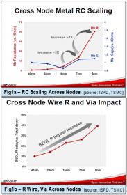 Similar to a fancy smartphone without a good wireless carrier quality (4G/LTE or 5G), a higher performance device is deemed an unattractive option as it needs to be accompanied by optimal wirings in order to minimize net delay attributed latency. Hence, to accurately measure design targets, capturing interconnect contribution during IC design implementation is crucial.
Challenges to parasitic extraction
From a designer’s standpoint, a good parasitic extraction solution should address accuracy, performance, capacity and integration aspects.
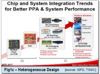
Accurate modeling of wire capacitances in an advanced node process is a non-trivial task as it is a function of its shape, context, distance from the substrate and to surrounding wires. It eventually leads to solving the electrostatic field in a region involving multiple dielectrics. The more heterogeneous design trend employing innovative and complex packaging has also necessitated the augmentation of existing extraction techniques with 3D-IC modeling capability (see figure 1c).
 As design size is growing, both the extraction file size and turn-around time increases –to reflect the jump in design net count, extracted RC networks size and its associated physical representation or layers handling. Capacity works both ways: the extraction tool of choice should be capable of absorbing a large design, do the extraction and produces an extraction file that is reasonably compact to be back-annotated in downstream timing analysis stage. All of these should be done fast, too.
Apart from managing route resources or interconnect (by means of pre-routes, layer assignments and route blockages), having an accurate and robust parasitic extraction technology is also essential in helping to pinpoint hot-spots due to ineffective utilization of wires or vias, and any potential signal integrity related issues. The extraction step should be interoperable with either the analysis or the optimization tools that will consume the parasitics data points.
Modeling, extraction accuracy and xACT
Both device and interconnect modelings hold critical role in providing accurate parasitic values. With device architecture transitioning to non-planar, multi-gate architecture such as FinFET and the upcoming the Gate All Around (GAA) structures, the current density and parasitic capacitance between the gate and source/drain terminals is expected to increase with further technology scaling.
During the micrometer process technology era, field-solver techniques for capacitance extraction was reserved for correlation purposes as it provided good results accuracy but was computationally expensive. We were also accustomed to labeling 2D, 2.5D, or pseudo-3D modes to RC extraction. Recently, there are many field-solvers and its variations noted (from finite element to boundary element based and to the most recent floating random-walk method). While accuracy is traditionally achieved through discretization of the parasitic equation by means of table lookup, such approach is inadequate with the increased layer and design complexity.
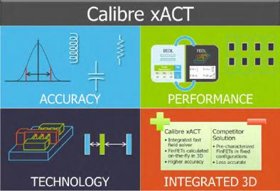
Calibre xACT™ is Mentor’s high-performance parasitic extraction solution. It combines fast, deterministic 3D field solver and accurate modeling of physical/electrical effects of complex structures/packaging used in advanced nodes –to deliver needed extraction accuracy, including rotationally invariant total and coupling capacitances.
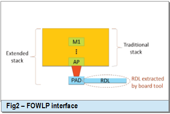 In order to address RC extraction of heterogeneous design such as a 3D-IC with FOWLP (Fan-Out Wafer-Level Packaging), xACT applies a 3D-IC modeling by taking into account two interface layers between the neighboring dies as shown in figure 2. It captures their interaction and creating an ‘in-context extraction’ which offers highly accurate and efficient extraction results –with 0.9% error and 0.8% for the total ground capacitance and total coupling capacitances, respectively.
xACT also handles new interconnect modeling requirements at all layers such as accounting potential shift in BEOL due to multi-patterning impact on coupling capacitance, MOL contact bias modeling, Line-End Modeling (LOM), etc.
Extraction size reduction techniques
SPEF/DSPF and log files are notoriously ranked top on IT’s disk-space screener list. These files though normally retained in a compressed format, are still huge and can strain not only disk space, but also downstream simulators’ capacity –so reducing the parasitic size while not losing the overall accuracy is key.
Unlike some parasitic extraction methods’ reliance on the use of threshold or tolerance value as basis for parasitic size reduction, xACT is resorting to a more efficient reduction mechanism known as TICER (TIme Constant Equilibration Reduction). Electrically-aware TICER produces a smaller RC network while controlling the error. This feature can be used across design flows (analog, full-custom and digital sign-off).
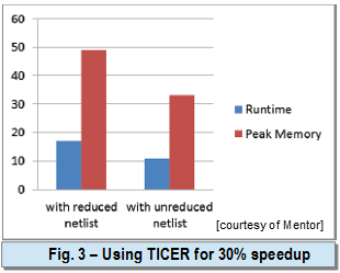
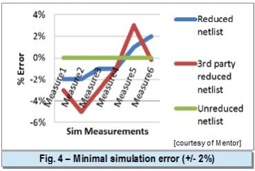 A trial on a 128K SRAM design shows 30% faster timing simulation a parasitic netlist with TICER reduction (figure 3) when compared to an unreduced netlist, while the simulation error was within 2% compared to the unreduced netlist (figure 4).
Multi-corner interconnect extraction is usually a requirement for cell characterization and design sign-off as they have to be performed across multiple process corners. The introduction of multi-patterning at advanced nodes adds even more corners. For example, due to multi-patterning at 7 nm, the original nine process corners gets expanded to more than a dozen, since each has one or more multi-patterning (MP) corners. Instead of running each process corner separately –which is costly, xACT performs simultaneous multi-corner extraction, in which all process, multi-patterning, and temperature corners are extracted in a single run. The user specifies the desired combination of corners to extract and netlist, which is done after a LVS run.
Speed, capacity and integration
Because designs are also growing in complexity at each successive node, a big challenge for parasitic extraction at 7nm is processing the design and the necessary corners without incurring additional cycle time during the signoff phase. xACT solution handles all of these complex modeling requirements and utilizes a net-based parallelism with multi-CPU processing to deliver fast and accurate RLC parasitic extraction netlists. It enables full-chip extraction of multi-million instance nanometer design with multi-threaded and distributed processing architecture.
Advanced technology scaling has also introduced increased geometrical variabilities induced by the uncertainties in the manufacturing processes. Such variations of the manufactured devices and interconnect structures may cause significant shift from their design intent –the electrical impact of such variability on both the adjoining devices and interconnects should be assessed and accounted for during signoff.
Performance is multidimensional. From implementation perspective, design performance is not a function of the characterized library and wire choices only, but might be influenced by signal integrity induced delay. On the other hand, reliability analysis such as EM and self-heating are becoming more common and augmented as part of sign-off, xACT provides device location information to these tools to ensure current density violations can be accurately identified and resolved. Subsequent corrective actions such as via doubling and wire spreading can be taken to reduce current density occurrence.
The Calibre xACT platform also uses foundry-qualified rule decks in the Calibre SVRF language, and is interoperable with the Calibre nmLVS™ tool and with industry-leading design implementation platforms.
For more details on Mentor’s Calibre xACT, please check HERE.
Share this post via:


Comments
There are no comments yet.
You must register or log in to view/post comments.