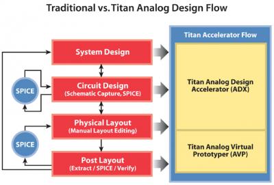
AMS design flows can follow a traditional path or consider trying something new. The traditional path goes along the following steps:
[LIST=1]
You probably noticed that there are iteration loops in the traditional flow after I’ve created a sized schematic or produced an IC layout. These loops take both precious CPU time and wall time, which means that your schedules tend to slip because you’re not meeting your specs soon enough.
There is another AMS design flow called model-based design that can reduce the time to design, optimize or port an IC design:
[LIST=1]
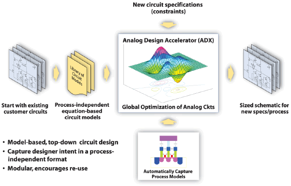
Magma has created this new AMS design flow and calls their tool the Titan Analog Design Accelerator (ADX). What strikes me most about this approach is that I’m not spending the majority of my time running circuit simulations and tweaking transistor sizes manually, instead I’m creating a model of my IC design using equations then asking an optimizer to do the hard work of creating the best sized schematic for me that meets the specification.
The design constraints for the analog optimizer could be:
- Area
- Power
- New specification
- Speed or frequency
- PVT corners
ADC Example
Using the model-based approach in Titan ADX an ADC circuit was designed then automatically optimized. The following plot has 11 different results from the optimizer showing Power versus Input Range in Red, then Active Area versus Input Range in blue.
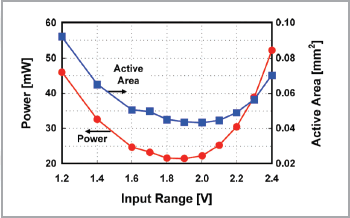
I can look at the trade-offs shown in the plot and then choose which of these 11 sized schematics to use. Both area and power are minimized around the 1.9V input range according to these results.
Optimizer Feedback
The analog optimizer provides plenty of info to help you make design tradeoffs:
- Sensitivity info for each constraint
- Constraints that limit design objectives most
- Critical PVT corners
- Floorplan constraints
- Layout constraints
Porting an IC Design
Let’s say that you wanted to port an AMS block from 130nm to 90nm. The following table will give you an idea of the time difference between a traditional flow and the newer model-based flow to port your design:
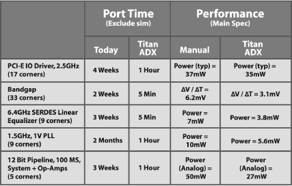
You still have to learn the new model-based design approach before you can start seeing results like this, so take that into account. Analog designers can be resistant to changing their methodologies however this new approach can provide your company with attractive time-saving and optimization benefits.
To get the most benefit from this Magma flow you have to add the Analog Virtual Prototyper (AVP) which lets you define the placement for your transistors.
Summary
If you are an AMS designer that wants an optimal IC schematic and layout sooner, then consider looking at the model-based approach offered by Magma called the Titan Analog Design Accelerator.


The Data Crisis is Unfolding – Are We Ready?