
At SEMICON West I attended the imec technology forum, multiple Tech Spot presentations and conducted a number of interviews relevant to advanced lithography and EUV. In this article I will summarize what I learned plus make some comments on the outlook for EUV.
Imec technology forum
As I previously published in a write-up of the 2018 SPIE Advanced Lithography conference, as EUV system performance has improved stochastics has become the main concern for introducing EUV into production. You can read my previous post here.
At the Imec Technology Forum Greg McIntyre, Direct of Advanced Patterning at imec presented “EUV Stochastics: Challenges & Solutions”.
The dose of an exposure is given by the number of photons multiplied by the photon energy, a Deep UV (DUV) photon has an energy of approximately 6.5eV and an Extreme UV (EUV) photon has an energy of approximately 91.6eV. In other words for the same dose there are approximately 14 times less EUV photons required. This makes EUV more prone to Shot noise and other stochastic problems.
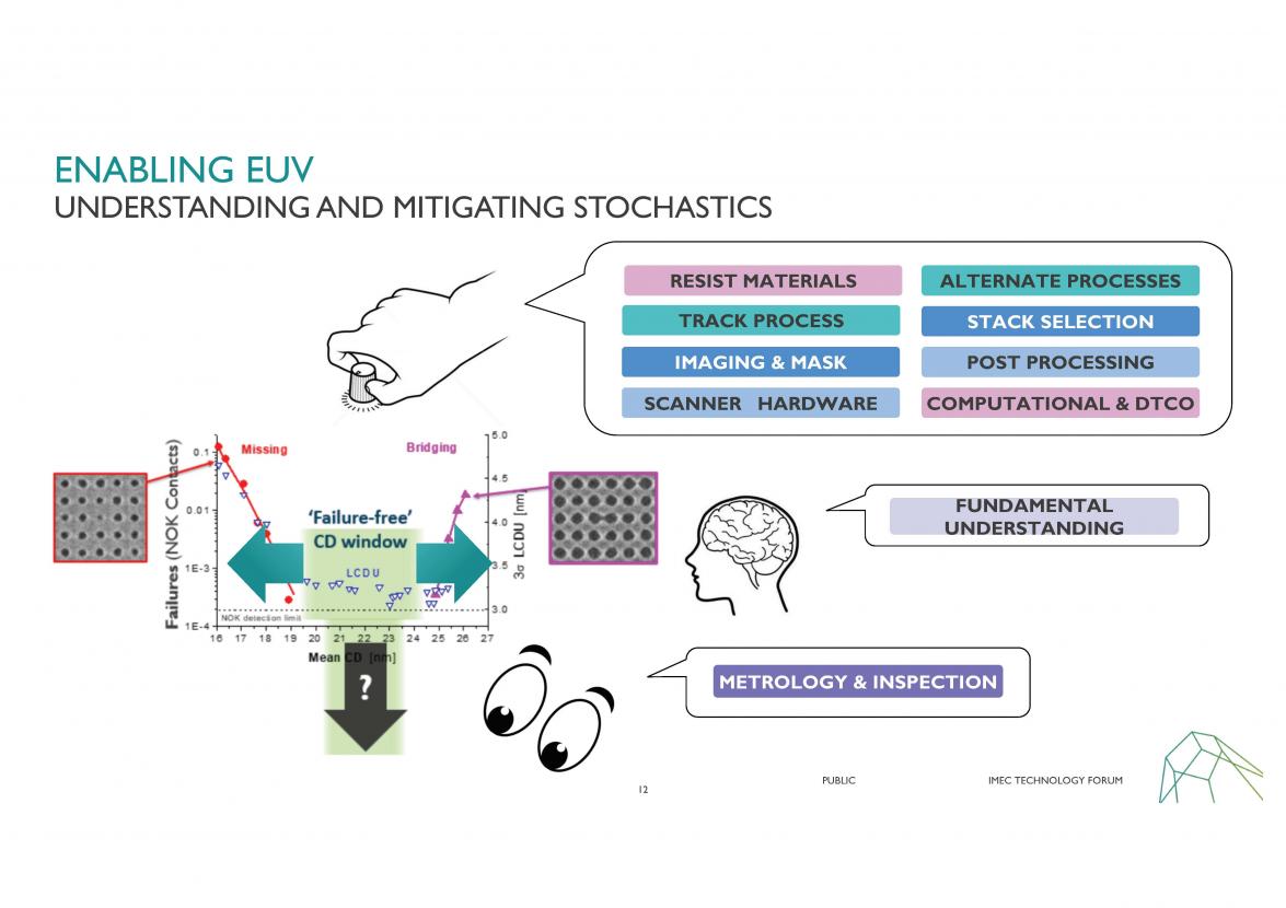
Imec is doing a lot of work to understand the fundamentals of EUV Stochastics in order to produce the widest possible failure free process window.
For example figure 1 illustrates the process window between missing and bridged contacts and some of the areas of investigation.
To-date the main dependencies identified are dose and CD but the photoresist polymer, underlayer, mask quality and exposure system pupil all contribute as well. See figure 2.
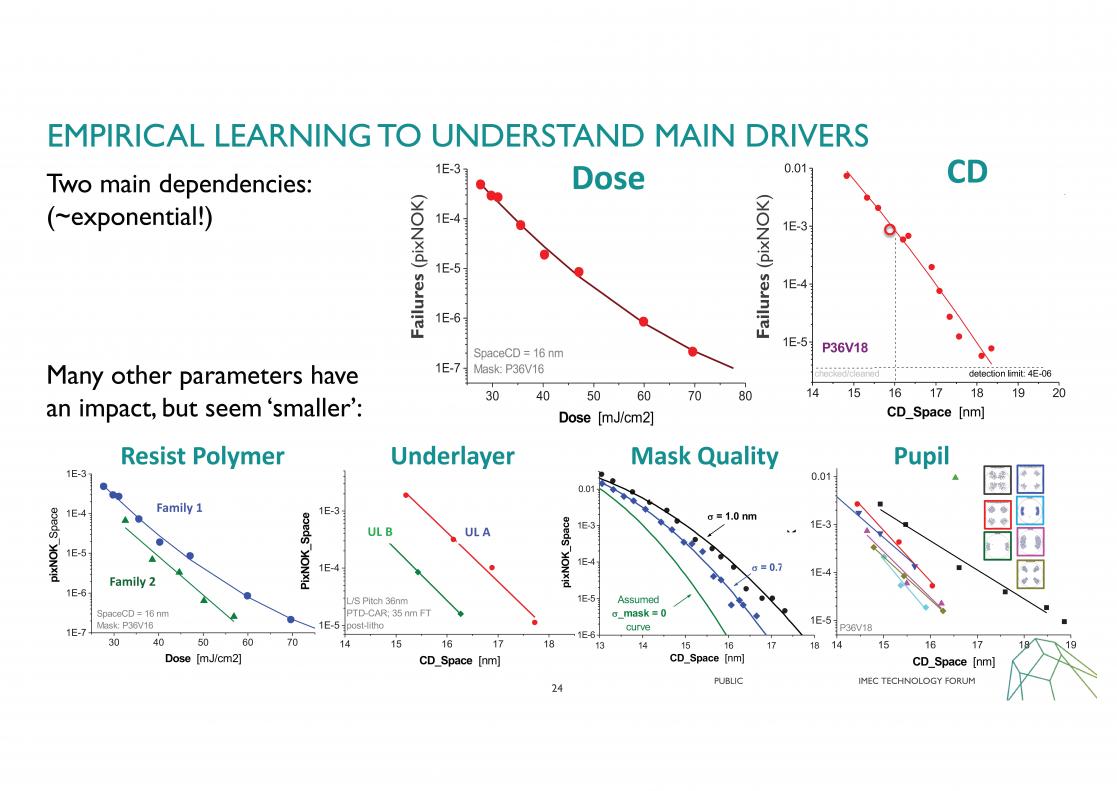
Figure 2. Empirical Learning to Understand Main Drivers.
Where DUV exposure reactions are well understood, EUV exposure reactions are less understood. In DUV, photons trigger chemical reactions, in EUV, photons primarily generate electrons that then trigger chemical reactions. In order to understand EUV exposure you need to understand how many electrons are generated, the energy distribution of the electrons and what chemical reactions occurs. Imec has brought a variety of advanced analysis techniques to bear on understanding the exposure reaction.
It has been found that EUV photons can directly scission the resist polymer and one question is whether to try to prevent this or use it as an exposure mechanism.
There is definitely a trend to simpler materials because the less materials you have in the resist the less variability you should have. Small – low variability molecules are also desirable.
Inpria is a novel metal oxide-based resist with a simple small block formulation that is getting a lot of attention (more on this later). Other options include adding metal sensitizers to chemically amplified resists to improve absorption, using E-beam type resists with polymer and no sensitizer and using EUV to scission the polymer or multi-trigger resist (I wrote about multi-trigger last year here).
In order for an EUV photon to generate a reaction it must be absorbed and the absorption rate is low in many resists (around 50% is ideal to maximize efficiency and also expose evenly throughput the resist), but simply increasing absorption doesn’t always translate to more sensitivity. Inpria absorbs 5x more photons than some other resist but needs more photons to do what it does so it isn’t 5x better.
Another area of intense research is smoothing the resist images to reduce line width roughness (LWR) or local CD uniformity (LCDU). Figure 3 illustrates some results in smoothing.
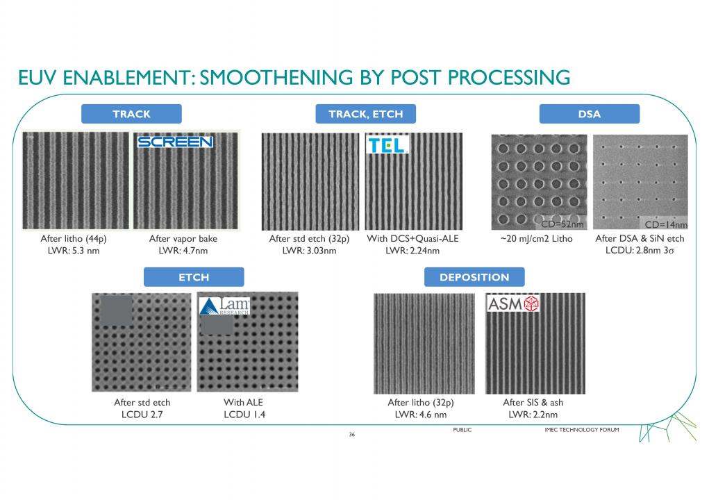
Smoothing is making good progress on all fronts in terms of understanding dependencies and capabilities. They need to make sure they can carry the smoothing throughout the hard mask. They want to not only smooth the pattern but also heal defects. Is using track smoothing with a solvent or vapor to locally melt the side walls in concert with etch technique better than just etch alone, is not known for sure yet.
Imec’s current focus is on providing good EUV performance for a 32nm pitch, as Greg explained it, the industry is currently ramping 36nm and Imec wants to be ahead of what is in production. One interesting side note, I mentioned to Greg I had heard TSMC is going to have a 28nm minimum metal pitch for their 5nm process next year and he immediately asked, single exposure? I replied that I hadn’t even considered that and what he told me was that a double exposure process with lower doses might actually be cheaper than a single exposure with high dose (more on dose later). EUV is a unique optimization problem because for DUV throughput didn’t change with dose within a reasonable window, but for EUV throughput is highly dose sensitive.
Inpria
I met with Andrew Grenville of Inpria during the show.
Andrew explained to me that one core principle for Inpria was to develop a targeted resist for EUV knowing stochastics would be a problem. There won’t be many photons so make a resist that absorbs the photons and do it with a simple structure. Andrew said they have the ability to get to 26nm pitch with reasonable photospeed, they can even go below 26nm but that is the tool limit. They can do 26nm pitch at 30mJ/cm[SUP]2[/SUP] but the defectivity is currently too high.
They are currently scaling up with a pilot plant to get to manufacturing, they are close to the rests being manufacturable.
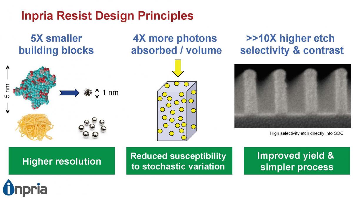
Inpria resist is built with metal oxide clusters based on tin because it has high absorbance, they are mid 30% absorbance and can go higher, 4 to 5x standard resists. The resist has small building blocks and no chemical amplification so no blur. They have gone to 8nm half pitch. Metal oxide is a very good etch barrier, so it can be very thin and opens up opportunities in the process window. All the clusters are the same, so you have a very uniform material. 10 clusters in just over 1 cubic nanometer so homogeneous on that scale. Stochastics are photon and material based, they have a very uniform film. Figure 4 illustrates the resist design principles.
The exposure reaction is absorbing photons creating an electron cascade within a short distance and then break bonds that allow a condensation reaction to occur. You get an efficient 3D network with few incident photons, you get a robust film with a high contrast solubility change. They designed the resist from the ground up to work in a photon limited regime. They can do a 32nm pitch with a 22mJ/cm[SUP]2[/SUP] dose and get <3nm LWR.
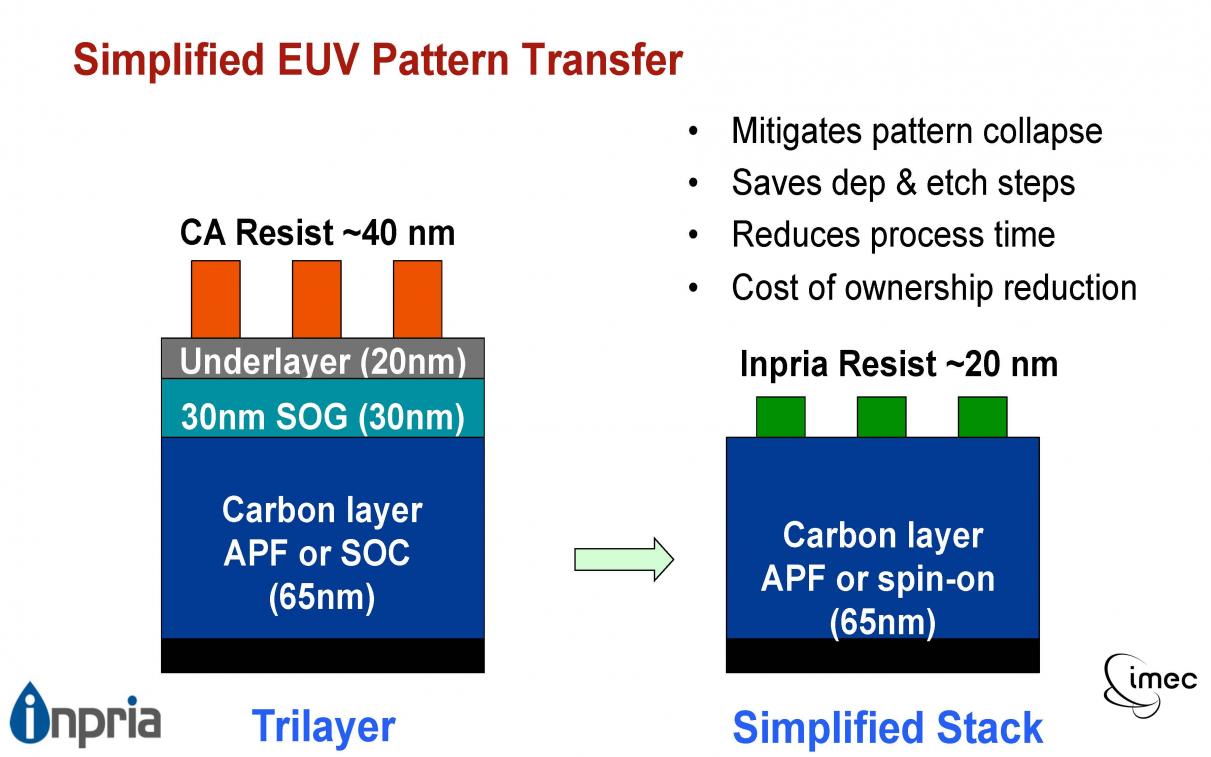
With chemically amplified resists (CAR) you need 2x the resist thickness over the under layers due to poor selectivity. Inpria has 100 to 1 to 40 to 1 selectivity to carbon layers. Figure 5 illustrates the simpler material stack needed with Inpria.
Another interesting comment is the they have more roughness at higher spatial frequencies that is easier to smooth. Traditional materials have lower frequency roughness that is harder to smooth. They can take a 3.5nm LWR in resist and go down to 2.4nm LWR in the hard mask. See figure 6.
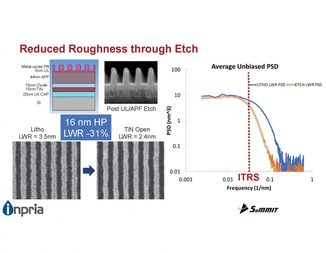
Figure 6. Reduced LWR through Etch.
Inpria is a negative resist but they can do easy tone reversals for block masks, contacts and vias. To remove the resist you don’t ash it but you can consume it in etching with Cl2, BCl3 etc. There are also fluorinated wet removal options depending on the under layer.
This is a story with many chapters, they are playing the long game. They are very bullish about their prospects in the long term.
Holistic lithography
Switching tracks a bit I met with Neal Callen of ASML to discuss their approach to holistic lithography. Neal is from the Brion side and involved in computational lithography to predict how masks will actually print. With the acquisition of HMI and their metrology tools he is now involved in the roadmap for HMI.
The HMI acquisition is the latest step in a longer-term strategy, ASML realized they needed access to good metrology. They invested in the tool to measure overlay and focus and feed it back to the scanner as opposed to trying to compete in metrology.
The tie in of Brion and HMI is interesting on multiple points. One, you can’t measure every wafer due to throughput constraints but modeling can help you know where and when to measure. Two, integration schemes with multi-patterning were starting to be driven by organizations outside of the photo group but they wanted to understand upstream. OPC models are developed two years ahead so modeling is a foot into that door plus computational modeling can be used for lens heating. Scanner performance with metrology and modeling to deliver the best patterns. Three, metrology today is typically measuring a monitoring feature in the scribe line but the challenge is does it represent what really happens on the die. They sell products that match anchor features to products.
Customers challenged them, why can’t we measure actual features, but there are billions of them, what do you model. With Brion their OPC model are large footprint so they use it to determine what features are most sensitive to dose or overlay. They provide a product to customers, so customers can determine what features to measure. To monitor their process. They can find features and know they are sensitive to focus and dose and overlay and they aren’t going to measure every die. The twin scan has a metrology chuck and an exposure chuck and they get focus and alignment data. They feed forward that information to their latest pattern fidelity tool and then quantify the pattern fidelity and determine whether the pattern matches what they want. The need to measure the feature, fast and many measurements and they need to find the feature in the die. So they bought HMI into the fold because they had the pieces needed. This wasn’t an attempt to get into the metrology market but rather because they wanted to close the loop.
They bring in a strategy not to just bring in a scanner, but an ecco system that is agnostics, the metrology systems have to be able to win on their own and then you put it together to deliver the best pattern through etch.
They are driving SEMs to have a resolution roadmap, and need to have speed. Multibeam is one approach, they presented a 3 x 3 beam at SPIE. Combine that with multibeam and make it faster and more intelligent and have driven order of magnitude improvements.
Their control strategy allows other metrology providers to create their own input parameters and feed it into the system. On the etch side they have a more cooperative approach in understanding how the pattern evolves through etch, work with etch companies or imec.
His organization trying to understand what shot noise really is and quantify. Is you have a missing contact and you pull back and really amp the area there is a signature, noise is only noise until you understand the signature that created it.
EUV Systems
I have seen a lot of comments about EUV systems and capacities with people trying to predict the number of exposures that can be achieved, I thought it would be useful to take a look at this.
Ignoring any alpha tools, ASML has shipped NXE3100, 3300, 3350 and 3400 systems. The NXE3100 systems are mostly decommissioned and can be ignored as a source of production exposures. ASML has shipped approximately 9 NXE3300 systems, 5 NXE3350 systems and 17 NXE3400 systems to-date. What is often ignored in discussions of production capacity is that the 3300 and 3350 systems can be field upgraded to 3400 systems and most of them are expected to be upgraded. The process of upgrading them is long and resource constrained and will likely take multiple years to complete but even assuming a four-year process, conversions can add 3 to 4 systems per year to the 3400 total.
By the end of 2018 the 17 NXE3400 systems already shipped should be on-line and possibly 1 conversion tool for a total of 18 tools.
The balance of 2018 should see 12 more systems shipped and the first half of 2019 should see approximately 15 systems shipped (ASML is expected to ship 30 systems in 2019). If you add in a couple of conversions in the first half and assume six months to get a system up and running after shipment, we could see an additional 29 systems on-line at the end of 2019 for 49 tools. In 2020 the balance of the 2019 systems should come on-line plus 20 systems shipped in the first half and possibly 6 conversion tools between 2019 and the first half of 2020 to yield 88 systems on-line.
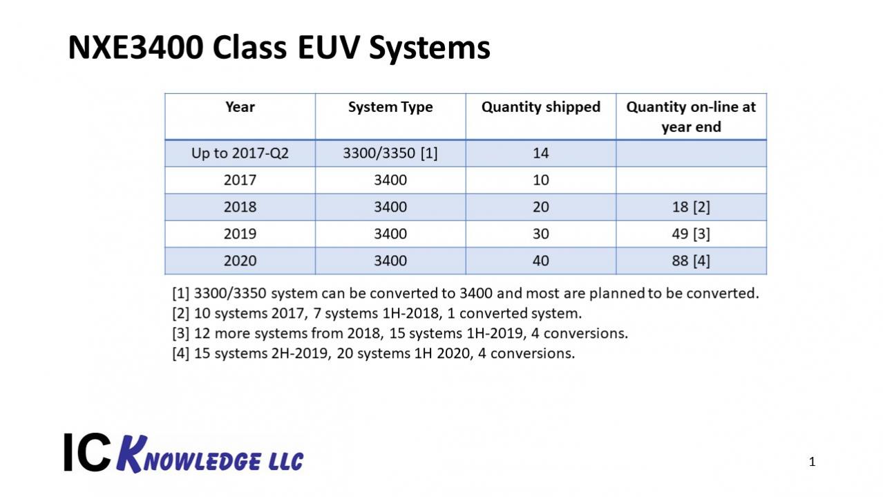
Figure 7. NXE3400 Class EUV Systems.
Samsung recently announced they are producing 1,000 wafers per day on their EUV systems. This is approximately 42 wafers per hour (wph). If we assume this is development and between uptime and utilization only operating 60% of the time, we get approximately 70 wph throughput. Based on ASML’s 140 wph announced throughput with 96 steps and a 20mJ/cm[SUP]2[/SUP] dose, and then correcting to 111 steps for logic wafers this implies a dose of approximately 45mJ/cm[SUP]2[/SUP]. The reports I have heard are that Samsung is running a 50mj/cm[SUP]2[/SUP] dose, so the math looks reasonable. Samsung has also said they are targeting 1,500 wpd for 2020. If we assume this is production with 80% for combined utilization and uptime, then we get 78 wph throughput and this implies a 38mJ/cm[SUP]2[/SUP] dose (I have also heard TSMC is working on a 40mJ/cm[SUP]2[/SUP] process).
Combining the systems forecast with the throughout data we can build a wafer forecast, see figure 8.
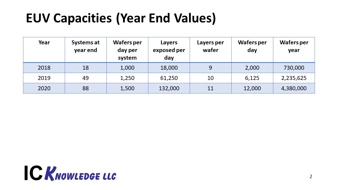
Figure 8. EUV Capacities (Year End Values).
At ISS in January I was invited to give a talk on “The Impact of EUV on the Semiconductor Supply Chain” and as part of that talk I predicted 900,000 EUV wafers would be exposed in 2019 and 2,075,000 wafers in 2020. With forecast EUV capacity of 730,000 wpy at the start of 2019 and 2,235,625 wpy at the end of 2019, to expose the 900,000 wafers forecast there should certainly be enough EUV exposure capacity. Similarly for 2020 the capacity at the start of the year is forecast to be 2,235,625 wpy and to end the year 4,380,000 wpy once again providing plenty of EUV exposure capacity to achieve the forecast. My ISS projection was based on estimated demand for logic wafers utilizing EUV and does not include any DRAM exposures.
My ISS talk write up is available here.
EUV Dose Versus Node
The industry is currently preparing to ramp EUV into production for the 7nm logic node with 36nm minimum metal pitches, but what about 5nm and 3nm processes.
Erik R. Hosler of GLOBALFOUNDRIES presented “EUV Lithography: The Next Generation” in a tech spot on Thursday.
Erik made a very important point that to keep a constant level of variation per photon, effective dose will need to double every node, see figure 9.
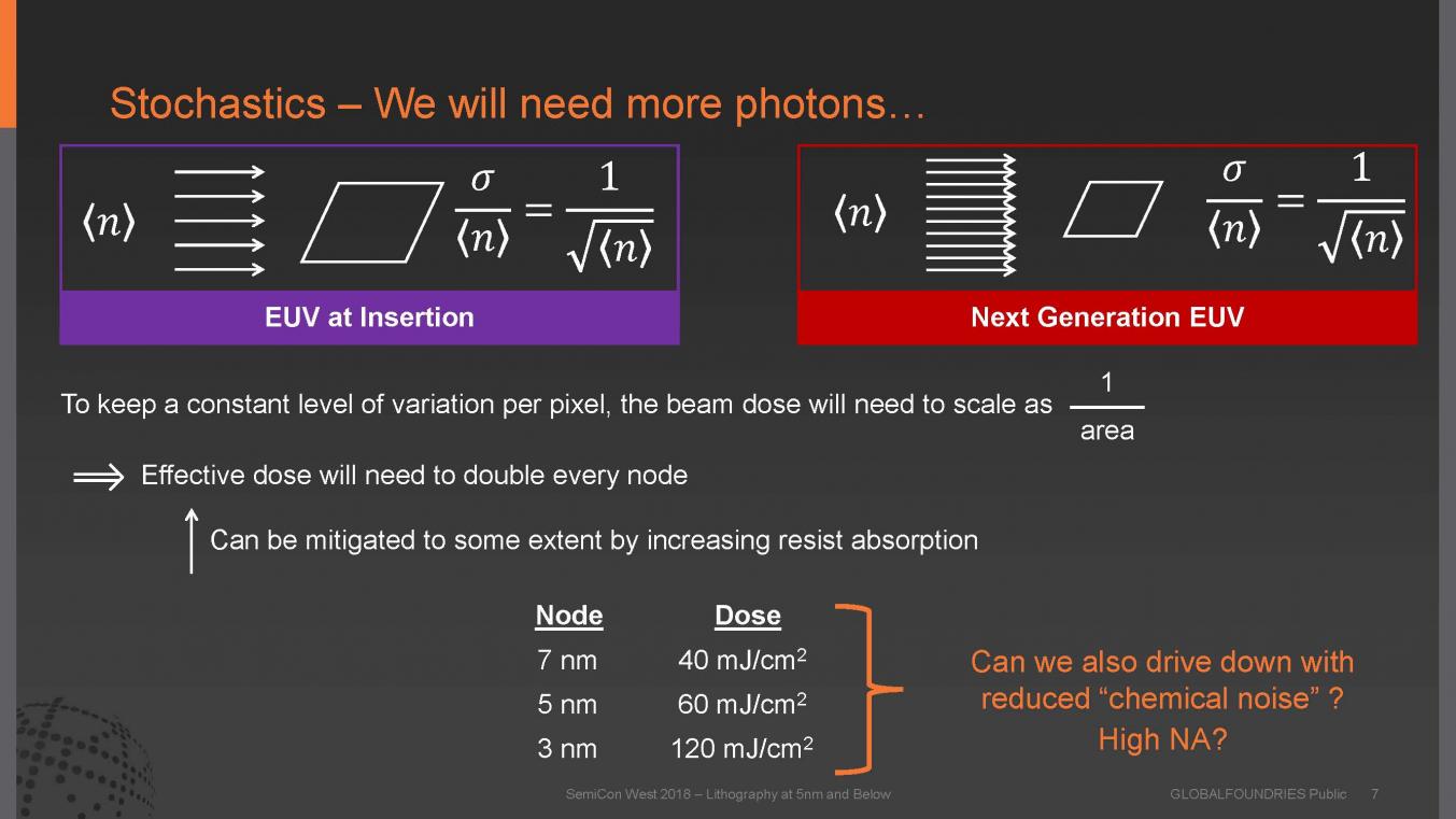
Similar to the Imec talk he noted that the molecular nature of matter is now relevant. We need resists with small and uniform building blocks. He talked about highly regular resists based on silsesquioxanes that are low noise, more absorbent resists based on metal oxides and chain scission resists for increased contrast and low noise. He touched on metal organic frameworks and click chemistry.
Today the goal is a 20mJ/cm[SUP]2[/SUP] dose for production but for future nodes we will likely have to confront higher doses and work to achieve sufficient productivity to be cost competitive.
Initial implementation of EUV has simplified OPC versus DUV but next generation EUV will require “OPC on steroids”. Model-based implementation of sub resolution features (SRAF) is already difficult in DUV, EUV adds additional complications.
Eventually EUV will need to transition to LEx or high numerical aperture systems. Erik presented an estimate that a high NA system could provide a 42% cost reduction over LELE with a standard EUV system.
Conclusion
EUV is poised to ramp into 7nm logic production over the next year. Continuing to extend EUV to 5nm and 3nm nodes faces a number of productivity, yield and cost challenges that require a better understanding of the exposure process down to the molecular level.


Comments
There are no comments yet.
You must register or log in to view/post comments.