
The projected revenue growth rate for IoT electronics remains strong, across a wide range of applications – e.g., visual object identification, voice recognition, machine automation, health and fitness applications, environmental and energy controls. A key component of these designs is the analog-to-digital conversion (ADC) functionality between the associated sensor(s) and the computational logic.
Synopsys has recently released an online webinar that provides insights into the architectural requirements and technical challenges for selecting ADC IP for IoT designs. Manuel Mota, Product Marketing Manager for Analog and Wireless IP, discusses the engineering tradeoffs for analog sensor data acquisition when developing an IoT solution.
IoT Electronics, Process Selection, and ADC Requirements
Manuel described a product differentiation in the IoT space, spanning from endpoint devices to sensor hubs.
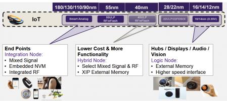
The endpoints impose very strict power dissipation limits, with implications on power management features required of the ADC. The cost and power constraints are driving integration of diverse IP. “55nm is the current sweet spot for IoT electronics. With the introduction of non-volatile memory at 40nm, that will soon emerge as the preferred node.”, Manuel indicated. At the other end of the spectrum, applications requiring high-performance computation are pursuing more aggressive process nodes – yet, there is still a requirement to integrate ADC IP for these sensor hubs.
ADC Architecture
There are several ADC architectures widely used – e.g., pipelined, flash comparators, successive approximation register (SAR), sigma-delta converters. “The SAR architecture is the appropriate choice for IoT designs, with the right balance between low power and high bandwidth.”, Manuel highlighted.
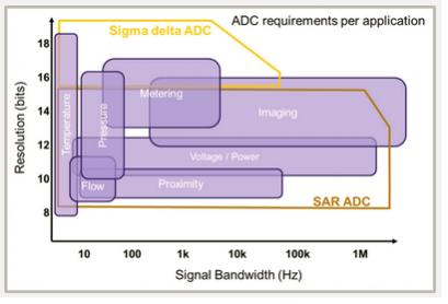
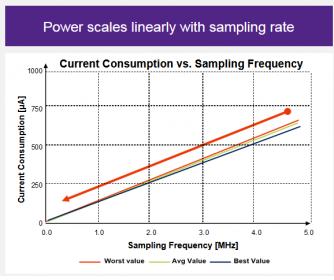
The power dissipation of an SAR ADC scales with the sampling rate. For many IoT applications, a moderate data conversion rate is sufficient, enabling power savings.
A block diagram of an SAR ADC is depicted below. The sampling of the sensor voltage input to the ADC is following by a succession of n comparisons for an n-bit register output. The control logic sequences through n cycles, where each bit of the SAR register is either set to ‘1’ or ‘0’, from MSB to LSB.
(From “Understanding SAR ADC’s”, Maxim Integrated Products, Inc.)
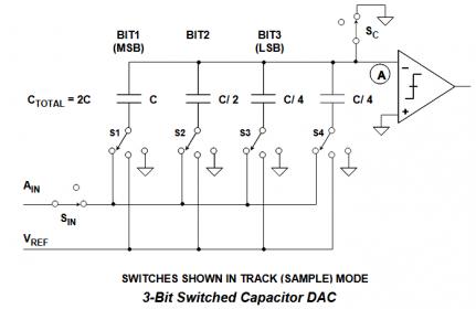
The key to the SAR is the internal n-bit digital-to-analog converter (DAC) implementation. For the first cycle, the SAR MSB register bit is set to ‘1’, all bits having previously been cleared. A corresponding voltage (Vref / 2) provided by the DAC is compared against the sampled sensor input voltage. Based on the comparator output, the MSB remains at ‘1’ (Vin > Vref/2) or reset to ‘0’ (Vin < Vref/2). The next cycle evaluates the (MSB-1) bit position in a similar manner, repeating the Vin versus DAC output voltage comparison down to the LSB. A simple 4-bit comparison sequence is shown below.
The critical feature of the SAR is the accuracy of the internal DAC. A simplified illustration is depicted below, illustrating the scaled capacitive array used by the DAC + comparator.
(From “ADC Architectures”, Analog Devices Tutorial MT-021)
During sampling, the sensor voltage is connected to all capacitors, charging the total capacitance to Vin. After acquisition, individual capacitors are toggled successively for each bit position, from MSB down to LSB. The scaling of each capacitance value provides a coupling event whose magnitude is a binary fraction of Vref, from 1/2 down to 1/(2**n). The comparator determines whether the coupled transition is greater or less than the original stored charge associated with the Vin sample. After the comparator settling time, the SAR register bit value either remains at ‘1’ or is reset to ‘0’ before evaluating the next bit position.
There are manufacturing variations associated with fabrication of the DAC capacitor array. The SAR control logic will likely include a calibration mode to provide error compensation. (For a novel implementation of SAR compensation, see reference [1].)
The SAR ADC IP will also likely integrate a low-dropout (LDO) voltage regulator, to isolate the IP from SoC supply noise.
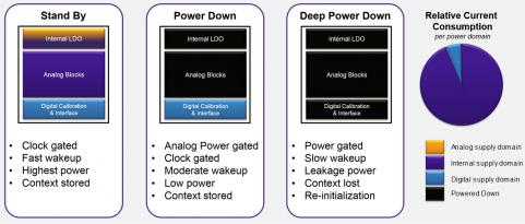
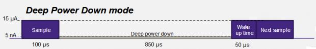
Manuel described additional power states implemented in the ADC, consistent with the focus on power dissipation reduction. The figure below illustrates power states ranging from simple control logic gating to a full deep sleep state, with a sample rate illustration including recalibration after power gating recovery.
IoT ADC Challenges
Manuel described some of the engineering tradeoffs for interfacing sensor(s) to the ADC.
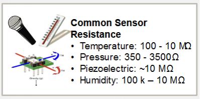
- sensor output resistance
High sensor output resistance results in a longer time constant to charge the ADC input capacitance – either a longer sample time is required, or buffering will need to be inserted between sensor and the ADC input, with impacts on IP area and power.
- sensor voltage excursion
Commonly, the Vref of the ADC is programmed to match the Vin voltage range of the sensor. However, a limited swing sensor may necessitate inserting an amplifier to achieve the desired resolution, with impacts to area, power, and Vin noise magnitude.
- sensor noise voltage
Speaking of sensor input noise, the IoT design implementation may opt to pursue oversampling to average out the input noise, if the sensor data acquisition rate allows.
ADC integration options
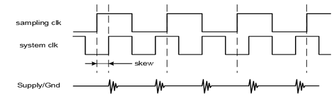
There are challenges associated with both the electrical and architectural integration of the ADC. Electrically, the ADC IP should be isolated from other noise sources on the SoC. An internal LDO provides supply isolation. Manuel also recommended paying attention to ground and substrate noise sources – one option was shifting the sample interval from the IoT SoC system clock, to minimize exposure to the ground bounce from digital switching activity.
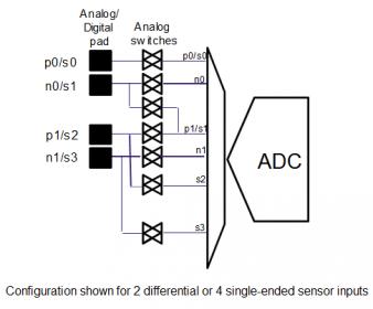
Architecturally, the IoT designer is faced with tradeoffs on SoC package pins, the number of sensors to observe, and (potentially) the need for very high-speed acquisition. Several topologies for sensor multiplexing and dual ADC’s for sample rate interleaving were shown.
There is an architectural design tradeoff on the ADC output, in terms of the internal bus traffic inside the SoC – the design may need to incorporate a local FIFO to store, then send burst data from the sensor(s).
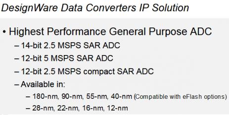
Synopsys offers a rich set of (silicon-proven) SAR ADC IP, with the requisite performance and power state support. I would encourage those interested in learning more about IoT sensor + ADC design requirements and challenges to view Manuel’s webinar, available at this link. (A simple registration process is required.)
-chipguy
Share this post via:


Comments
There are no comments yet.
You must register or log in to view/post comments.