
I am sure there are many FPGA designers who are quite content to rely on hardware vendor tools to define, check, implement and burn their FPGAs, and who prefer to test in-system to validate functionality. But that approach is unlikely to work when you’re building on the big SoC platforms – Zynq, Arria and even the big non-SoC devices. It would simply take too long to converge functionality and performance. As usual, expectations keep ramping up – 400MHz performance, shorter design cycles and more designs per year, driving more reuse but still needing to meet the same regulatory and/or safety requirements. Sounds a lot like ASIC/SoC demands (except for GHz speeds in ASIC). Unsurprisingly, FPGA designers are turning to similar flows to manage these demands.
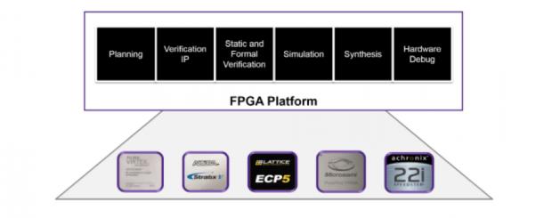
The design steps should look very familiar: planning, IP verification, full design static and formal verification, simulation, synthesis, implementation and hardware debug. Like the ASIC folks you may want a second-source option, in which case this flow needs to be able to target multiple FPGA platforms.
Planning is common in both domains, but here it must be much more tightly tied to pre-silicon functional verification. If you have to signoff to DO-254, ISO 26262, IEC 61508 or other requirements, you already know you have to demonstrate traceability between testing and specs, and completeness of testing. Which means you need linkages and as much automated correlation as possible between documents, testing activities, bug tracking, testing coverage, static code compliance metrics, and so on.
Many FPGA designers are already familiar with static verification, an elaborated version of the linting of 15+ years ago. This is still a mainstay and a requirement in many FPGA flows (DO-254 for example mandates a set of coding-style rules). Equally important here are clock-domain crossing checks. A big FPGA may host 10 or more clock domains and 10k+ clock domain crossings. If you don’t use static analysis to find and check these, you face a lot of painful debug on the board. The better static checkers do a comprehensive job in finding all crossings, while reducing the cases you have to analyze to a digestible format.
Formal verification is a newer entrant in FPGA verification but is gaining ground for some fairly obvious reasons. One is getting to acceptable code coverage. All big designs have unreachable code – from disabled or forgotten functionality in legacy or 3[SUP]rd[/SUP]-party IP. You can’t hit this in testing no matter how hard you try, but it’s still going to damage your coverage metrics unless you flag the code to be excluded. That’s not always so easy, especially if you don’t know the code. Fortunately, there are formal methods which will search for unreachable code, and will automatically create those exclusion commands.
Formal adds more capabilities through “apps” for the formal novice, such as looking for inaccessible states in FSMs or design exploration apps which will help you probe characteristics of your design without need to setup complex testbenches. In general formal can be a very valuable complement to simulation, for what-if experiments and when you want to be sure something can never happen, say in a complex control system where multiple FSMs are interacting (that’s a topic for more advanced formal users, but remember this if you run into such a problem).
The heart of verification in these flows is still simulation, which has evolved a lot from earlier simulators. Now it has to be mixed language, Verilog, VHDL and SystemC, modeling all the way from TLM through RTL and gate-level. These are big designs running at least some level of software on ARM cores, so you need all the acceleration you can get through multi-core and other techniques.
For testbenches these days you should be looking at UVM along with (SystemVerilog) assertion support and management, because you should be using assertion-based verification anyway but also because your IP and VIP will be loaded with assertions. And your simulator should provide strong constrained-random support with an excellent constraint solver, since you’re going to depend heavily on this for coverage.
Something that may be new for some FPGA teams is the need for good VIP (verification IP) in your verification plan. A lot of what you will be testing with interacts with standard protocols – the many flavors of AMBA, PCIe, USB and so on through the alphabet soup. VIP provide proven models for the testbench to simulate traffic under many possible conditions. You’ll need these not only for testing functionality but also for performance testing. Will your design hold up under heavy traffic?
You also need a very good debugger, which now has to support protocol transaction views in addition to the traditional signal waveform kinds of view. You don’t have the time or probably the expertise to figure out what’s broken in a protocol at the signal level; the right place to start looking is at the transaction level. Incidentally you really need for the same debugger to support simulation, formal and static verification, for ease of learning certainly but also for integration between the different types of verification and coverage.
Finally, what can the flow vendor do to help you in post-silicon debug and better still, bring that debug data back for drill down in the flow you used to verify pre-silicon? Again the FPGA vendors provide logic analyzer capabilities here but likely not as well-integrated with the pre-silicon flow. So that’s consideration if you think you may need to do some tracing through the RTL. When looking for a debug solution it should be easy to use and integrate easily with the verification flows for quicker turnaround times.
The flow needs a good synthesis engine. Why not just use the FPGA tools synthesis? You can; naturally they understand their underlying architecture as well as anyone, so you can expect they will do a good job in optimizing your design to the hardware. But they’ll freely acknowledge that they don’t synthesize to competing platforms and they don’t have the depth and breadth in synthesis technologies that you’ll find in the big EDA companies. Which is why they work with those companies to enable those EDA tools to also optimize on their FPGA platforms with high QoR, advanced debug and deep verification.
I haven’t talked about any preferred solution in this blog; ultimately you should decide that for yourself. But I think I have described a reasonable checklist you might want to use to grade solutions. One possible solution is described in this webinar.
Share this post via:


Comments
There are no comments yet.
You must register or log in to view/post comments.