
At the Imec technology forum in Belgium Gouri Sankar Kar and Arnaud Furnemont presented memory and storage perspectives and I also got to interview Arnaud. Arnaud leads overall memory development at Imec and personally leads NAND and DNA research.
Memory research is focused on power, energy, speed and cost with energy and throughput presenting particular challenges.
In 2018 it is estimated that approximately 30 zetabytes of data will be generated, by 2020 it is expected that 50 zetabytes of data will be generated annually and in 2025 nearly 160 zetabytes annually.
Data center energy consumption is growing so rapidly that by 2030 data centers may use as much energy as Europe, Africa and much of Asia do today.
To-date Flash memory density has been keeping pace with the increases in data but with the transition to 3D NAND the log trend cannot be maintained. Energy and speed are far from keeping up with the data growth rate (see figure 1).
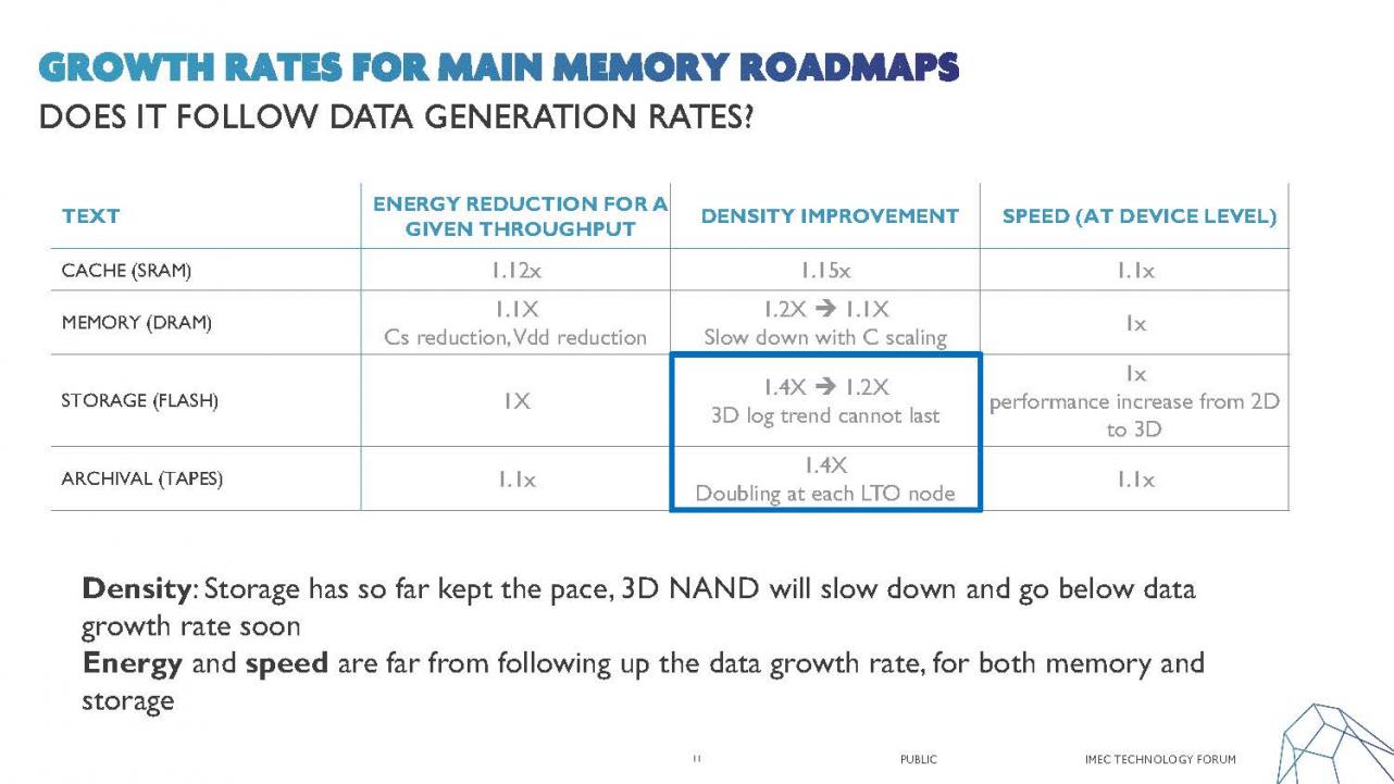
Figure 1. Growth rates for main memory roadmaps
SRAM and cache
For cache memory Imec is working on MRAM. STT MRAM can replace SRAM for L3 cache and shows an almost 80% reduction in energy. For L2 and below cache, where greater speed is needed Imec is working on spin orbit torque MRAM. MRAM can be formed in the interconnect layers over logic potentially reducing die area as well.
DRAM
Continued scaling of DRAM is becoming very difficult. DRAM storage capacitors used to have 20 to 25 fF of capacitance but today at the leading edge are down to 10 fF. This has required optimization of the bit line capacitance and correction code.
Roughly one half of a DRAM die is peripheral CMOS. Over the long term a move to high-k metal gates and FinFETs is expected to shrink the area.
Capacitor spacings are becoming so tight that cylinder capacitors with dielectric on the outside and in the center of the cylinder will give way to pillar capacitors with dielectric on the outside only due to spacing limitations. This change may make it possible to use thicker films of higher-k dielectrics. There is a fundamental trade-off between k value and leakage with the higher k films leaking more but a thicker layer could potentially overcome this and allow a different k value versus leakage optimization.
If a deposited thin film access transistor can be developed it may be possible to put the access transistor and capacitor over the peripheral CMOS increasing density.
Figure 2 illustrates the Imec DRAM roadmap.
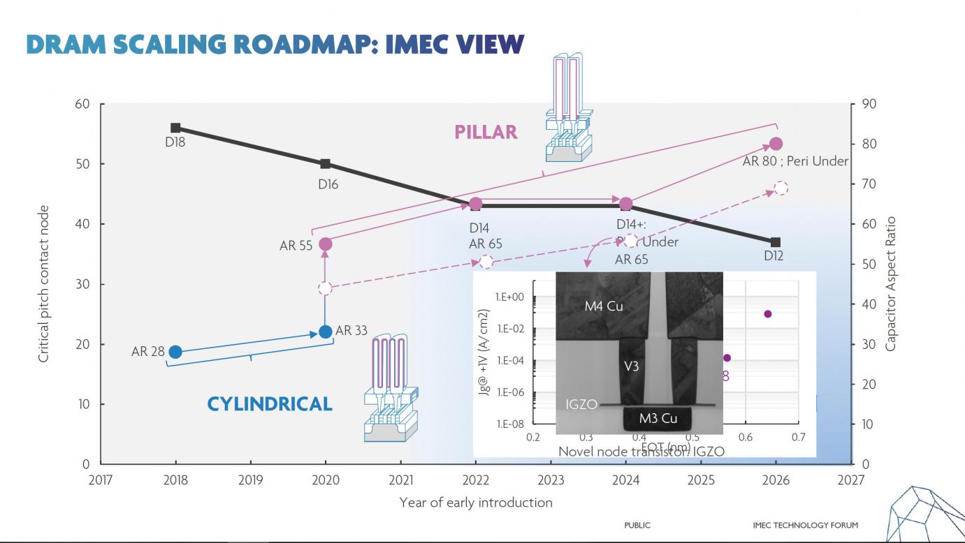
Figure 2. DRAM Scaling Roadmap: Imec view
DRAM density scaling has slowed to ~1.1x per year.
NAND
2D NAND followed an exponential trend with a doubling in density per node but now 3D NAND will provide slower scaling as early double of layers becomes 1.5x and 1.33x layer increases per node.
3D NAND is transitioning to 4 bits per cell from 3 bits per cell. Peripheral CMOS under the memory array such as Intel-Micron is doing should become more prevalent but will require changes for Samsung and Toshiba who currently create epitaxial select transistors in the substrate.
String stacking has been implemented by Intel-Micron where one half of the memory array layers are put down, the channel is formed and then the second half is deposited, and the channel finished. Because Intel-Micron is a polysilicon-oxide stack that is difficult to etch they had to string stack first but Samsung and Toshiba will eventually need to string stack as well. Intel-micron may eventually need to move away from polysilicon-oxide stack based floating gate to charge traps cells based on oxide-nitride.
As the number of layers increases and the stack height grow the height of the vertical channel will require a change from polysilicon to silicon germanium and eventually III-V materials for lower resistance.
As the number of memory array layers increases the array thickness will approach the thickness of the die requiring careful stress control and optimized layer thicknesses.
Figure 3 illustrates Imec’s 3D NAND memory roadmap.
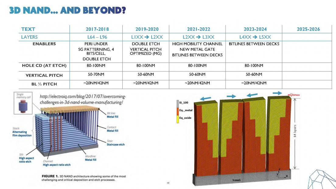
Figure 3. 3D NAND …. And Beyond
DNA
In the longer term Imec is investigating DNA for storage. DNA is very dense with >>1Tb/cm2 and in a 3D storage structure all the data in the world could fit in your car. DNA is very stable with biologists planning to bring back the woolly mammoth in 2019. Imec’s goal is to make it cost effective.
Conclusion
MRAM offers a lot of promise as a replacement for SRAM in cache applications. DRAM scaling is slowing and approaching fundamental limits. 3D NAND offers a NAND scaling path but will be slower than 2D NAND was delivering. In the long term DNA may offer the ultimate in archival storage density.


The Data Crisis is Unfolding – Are We Ready?