
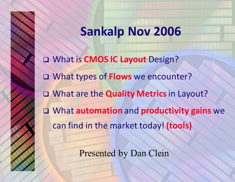
 The year is 2005 and PMC Sierra decided that it is time to expand by adding a new site in Bangalore, India. We started with digital verification first but by 2006 we were ready to engage with Mixed Signal Design and Layout. I went to Bangalore in June 2006 for the first time and with the help of our local manager, Vikram Labhe, had a few layout services companies come and present their competence. Started with Wipro, SiCon, then Smartplay and Sankalp. After 2 weeks of meetings and interviews I decided that the best bet for PMC was Sankalp. The main reason was that their growth plan was “organic from inside” without stealing people from other companies, fact of pride for the other contenders. I met the management team, Vivek Pawar, Mrinal Das, Alok Pugalia, Prabhat Agarval, and Mohan R. Their dream was to build a service company by taking new grads and train them into solid layout designers. More than that, they decided to build design services centers in second tier cities attached to second tier universities, which will raise the level of these locations and their population.
This was also a good business idea from the point of retention compare to big cities like Bangalore, Noida, etc. As a person who already trained a “few” generations of layout designers in different 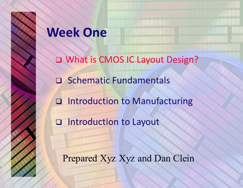 countries this was “music to my ears”. I visited Sankalp sites and got 2 bright people with little layout experience but a lot of enthusiasm. Now we wanted to grow our Bangalore PMC Sierra team but also the Sankalp team working with us. If I wanted to get more knowledgeable people for my team I had to get involved in their training. I started by reviewing Sankalp materials and decided that they needed help. I took my Cadence 5 days training course and made it 5 weeks for new grads. As the students already had electrical knowledge I had to adjust a few things but with the help of Sankalp future trainers we got the ball rolling. Using Mohan analog experience, Alok memory expertise and Prabhat IO and design knowledge we ended up with a great material that covers 2 months training.
For the next 5 years I had sessions with all new students on tools and methodologies, and yes long nights and SKYPE video were part of the norm… But the results were astonishing and we were able to pick up the best students for our PMC team. Using these updated materials and contributions from Vivek, Mrinal and other external advisors, Sankalp trained from 2007 until today more than 1200 new grads, so I consider  my time “well spent”.
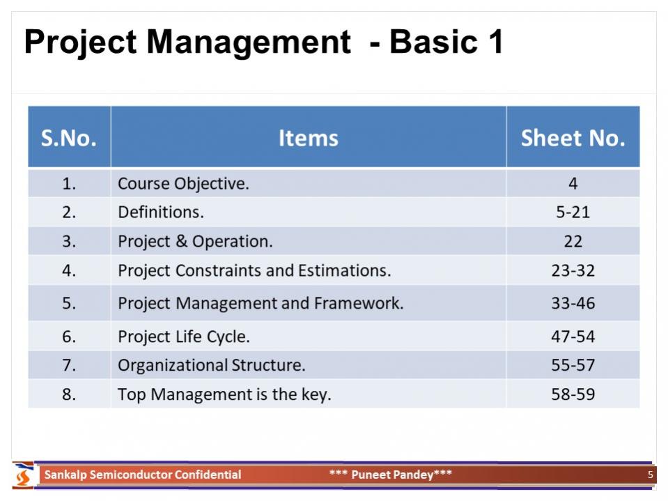
I wrote and delivered in the following years a few more training for Sankalp: a Train the Trainer for the teachers of the course, an Introduction to Management and Project Management for new leaders, and helped the soft skills teachers prepare a few other courses. Later in Sankalp we developed Project management with Puneet Pandey and a lot of soft skills materials with Shilpa HP and Bhuvaneshwari Shurpali, the trainer in ekLakshya. I visited India every 6 months and all my weekends were training classes for Sankalp employees, new grads or experienced. As I said before, training was and it is, one of my favourite activities  even so it was for food and board 😊

In 2013 when PMC Sierra decided to ramp down the layout team in North America I had to look for something else interesting to do. As Sankalp was my account from 2007 I knew the management, the infrastructure and most of the people, around 500 at that time. I figured that I can rebuilt some of the layout capabilities in Canada but I needed help from a low cost & big size partner. The obvious option was to join Sankalp and start a Canadian office in Ottawa.
All good but I cannot do only management and business, needed to get back to the “fun” activities: tools, flows, mentoring and training. One of the activities I am very proud of started with Mohan R and Sati Patil, the only CAD guy in 2013. We wanted to improve Sankalp productivity and grow people interest in automation. So we put together a plan:
1. First Sati built an internal Central CAD website where we uploaded all possible training materials we could find. DAC proceedings, CDN Live papers, vendors tools manuals, white papers, etc.
2. We worked on specialised training materials for CAD people so we can grow the group, organic again. We developed a full ticketing system to ensure the voice of inventors and innovators is recorded and addressed. This work helped building a new breed of experts with scripting skills, not only layout or design. Today Sati has more than 40 people in automation…
3. We agreed that the biggest ROI for an internal automation is “migration”. A lot of customers came to Sankalp and asked for small modifications, derivatives of IP or just IP migration between processes in the same technology node or different.
4. We also wanted to solve another Sankalp reality: even so our trainees for all specialties were much better prepared than other new grads or juniors, all customers wanted people with 2+ years’ experience in their projects.
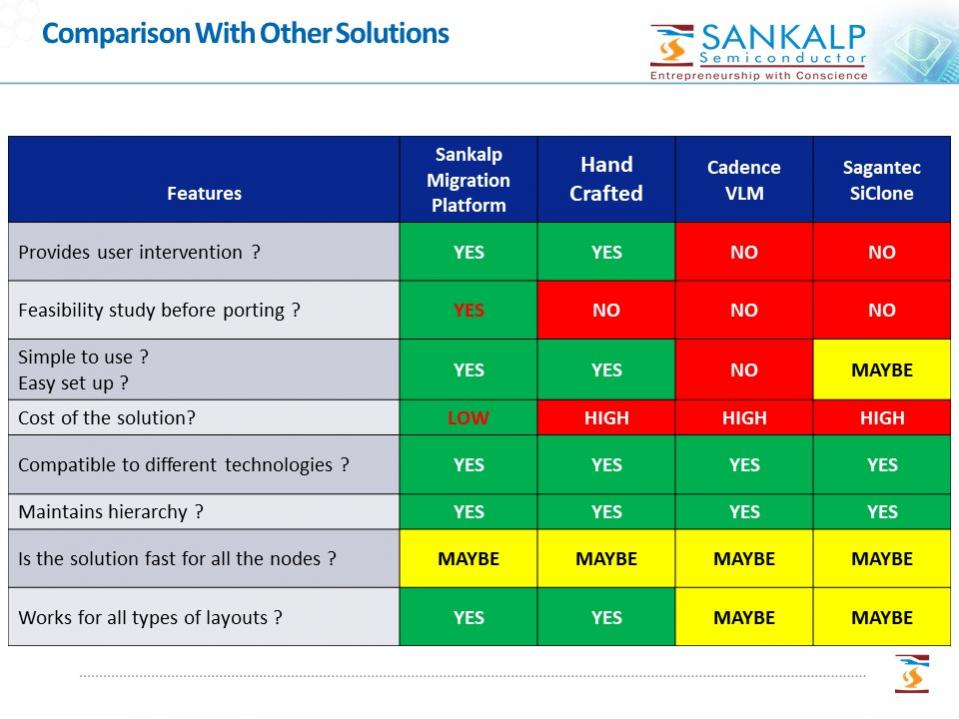
5. Based on my personal knowledge on “compaction & migration” tools (Rubicad, Sagantec, Magma, Qdesign (Cadence VLM), etc.) I knew that we cannot succeed where more money and better trained resources failed.
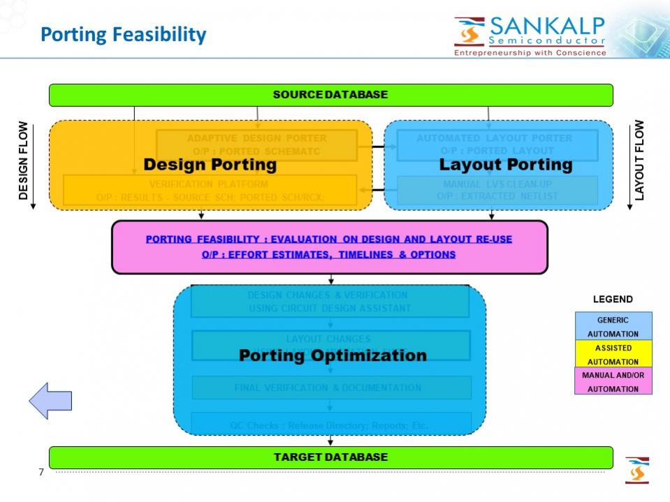
We decided to build a Platform (not a software) for IP Process Migration.
 I worked with 3 people: Sati Patil for CAD, Sumit Bhat for Circuit Design and Uday Pendse for Layout. For about 1 month we had brainstorming sessions to figure out the flow and then decided to put everything in a “marketing presentation” so Mrinal Das can review and approve project development and budget. We had options and processes, efforts and schedules so once we got the green light the team hit the ground running.
Sankalp can migrate analog/full custom IP today (not digital standard cell blocks or memories) and we can also help the customer make decisions. While in PMC we asked service providers if our blocks are migrate-able and the answer was always “sure”. It most cases proved to be wrong so I wanted a feasibility gate in this migration platform.
What is Sankalp Migration platform : and entire environment that contains scripts, decision points, built around CADENCE software, verification tools and a lot of manual labour. Tools cannot solve more than 80% of technology design rules so we are using the 0-2 years’ experience juniors with a few experts to bring the results to 100% compliance DRC and LVS and performance. This way they get experience in various technologies, different designs, etc. which makes them better prepared for customer challenges and we have a new business offer.
The biggest novelty is the feasibility. We are able to provide of migrate-ability factors to each IP candidate for migration.
 1. Simple design rules changes – no layout architecture change (generally for same node different vendors)
2. Design rules changes that will require some layout architecture changes – process node size difference (resistors, capacitors, inductors, etc., do not change linearly with process size)
3. There are design rules limitations that impact circuit design so a circuit modification will be needed including new simulations and ECO – the case of different type of devices not available in destination process – little circuit design and a lot of layout
4. The new process has many different device options, electromigration and RC variants, etc. – a lot of circuit design changes and a lot of layout work but the circuit can me modified
5. Non migrate-able – circuits with inductors, VCO, LNA, big process variation that will require redesign
We can provide all these 5 “migration factors” including effort estimation for each and if customer decides to give Sankalp the job, we can implemented all options internally. I am very happy with this new platform that has 2 years and was used in many engagements, some complete solution and some partial as automation is useful to reduce any design effort. Not only that but parts of this platform automation is used in a variety of projects to improve team productivity.
On the other front, slowly but surely I am working with some of my industry friends to my second edition of CMOS IC Layoutbook planned to bereleased by end of 2018!
The conclusion I want the readers to take home after these 10 articles:
If you are a layout designer who just entered in the industry and wonder what else you can do, look around. Opportunities are everywhere if you want to expand your knowledge, get engaged into other activities related or not to Layout (of polygons), and have fun.
Never wait for others to offer (give, teach) you to grow, go do it on your own, I did!
I started layout in 24 January 1984 and still have fun today!
If you have ideas and would like an advice my email is cometic@ieee.org
If you want to talk to me face to face please visit Sankalp Booth 2457 at DAC 2018 in San Francisco.
Dan Clein
Share this post via:


The Data Crisis is Unfolding – Are We Ready?