
I was invited to give a talk at the Business of Cleans Conference held by Linx Consulting in Boston on April 9th. I am not a cleans expert but rather was invited more to give an overview talk on process technology trends and the impact on cleans. In this write up I will discuss my presentation. I discussed each of the three main leading-edge technology segments, DRAM, Logic and NAND.
DRAM
In my first DRAM slide I present the DRAM nodes by company and year. Micron Technology, Samsung and SK Hynix dominate the DRAM market and I present the nodes for all three companies. DRAM nodes are currently defined based on the smallest half-pitch on the devices, for Micron this is the word line and for Samsung and SK Hynix is based on active.
Underneath the chart are some images of key technology developments. On the left side, the saddle fin access transistor with buried word line is shown. The saddle fin with buried word line is the current standard for access transistors. On the middle and bottom right, the evolution of DRAM capacitors to finer pitch – high aspect ratio structures is shown.
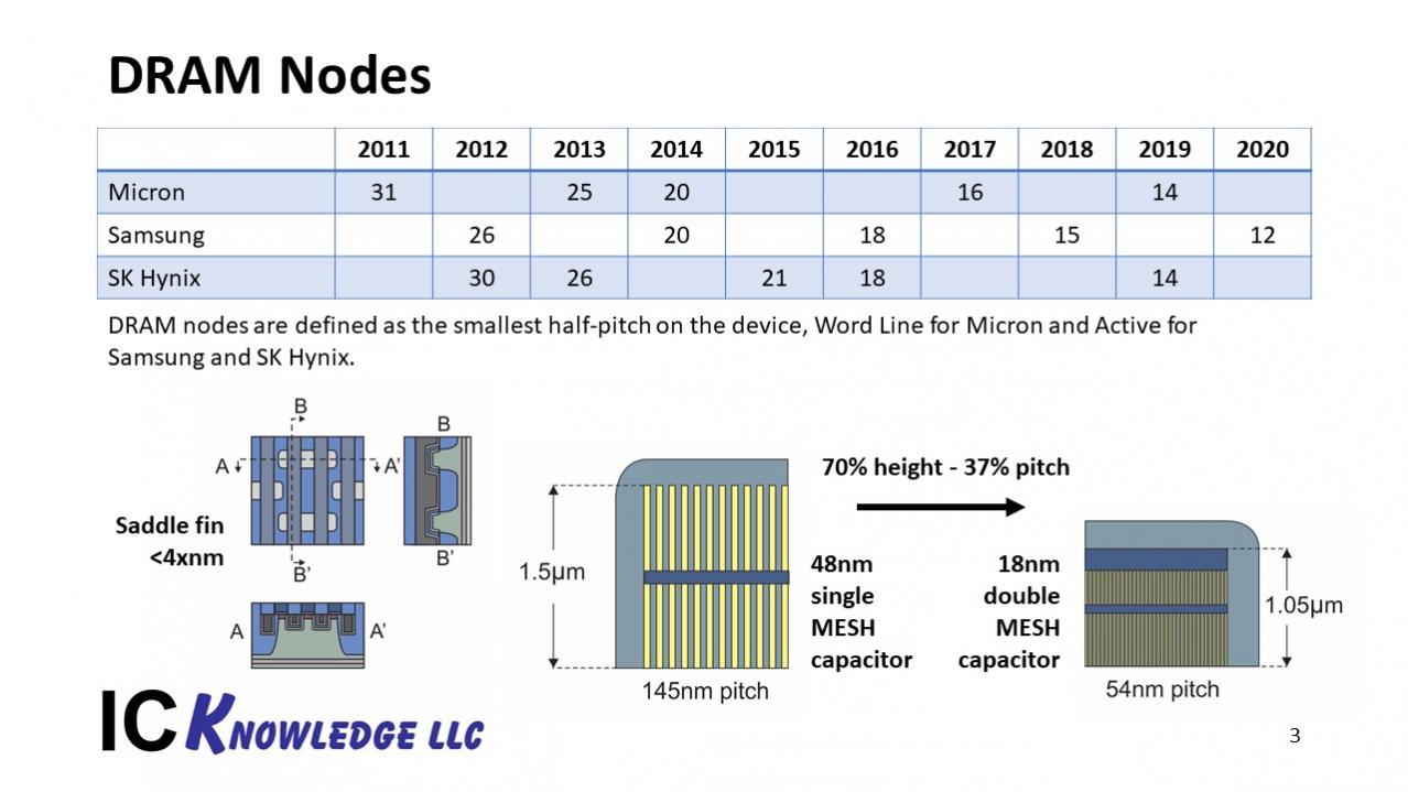
Presentation slide 3. DRAM Nodes
The key issue with DRAM scaling is the capacitor. A minimum capacitance value is required in order reliably store a bit. To continue to create capacitors that take up less area on the chip the capacitors can get taller, the film can get thinner, and, or the k value of the film can increase. The problem is the capacitors are as tall and thin as can be reliably produced from a mechanical stability stand point, the film thickness can’t be reduced any further without leakage issues and as the k value of the film increases the band gap decreases also leading to leakage issues. Composite films of aluminum-based oxide for low leakage and zirconium-based films for high k values have become the current standard and it isn’t clear there is a better alternative.
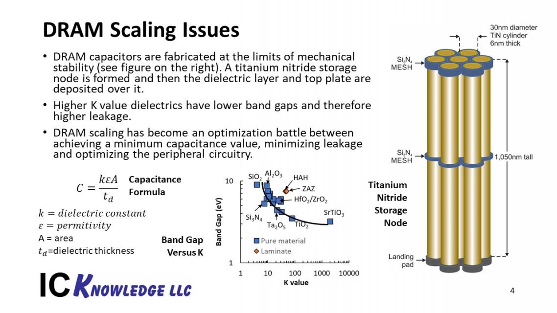
Presentation slide 4. DRAM Scaling Issues
In slides 5 and 6 I go through some of the major DRAM process blocks and discuss the clean and wet strip needs.
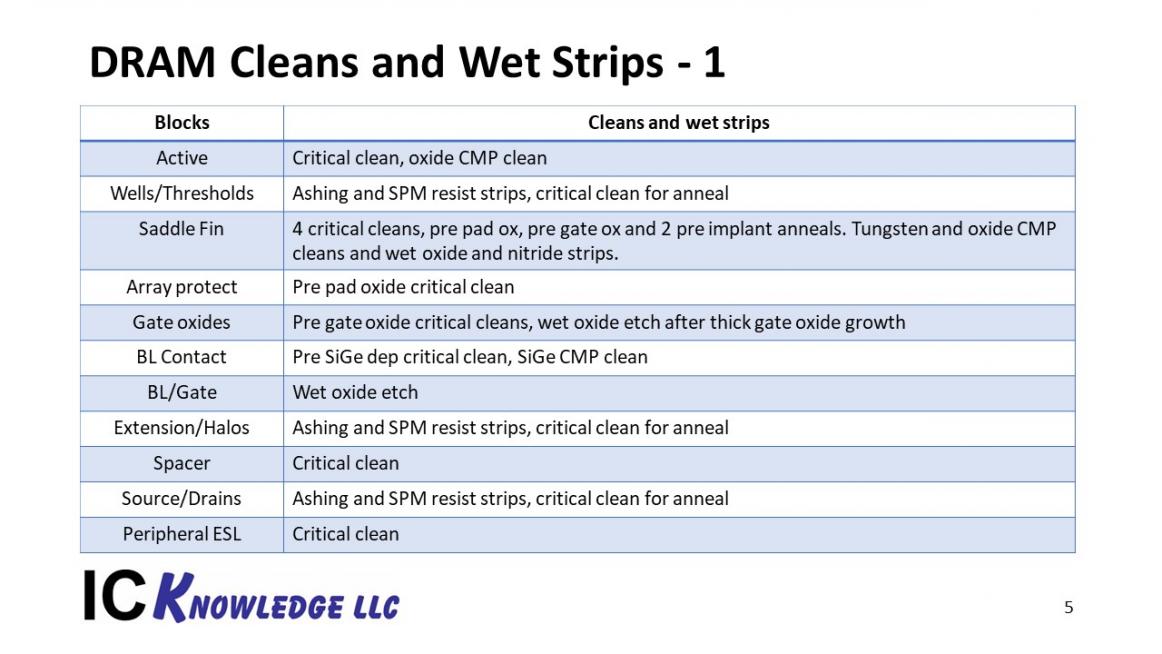
Presentation slide 5. DRAM Cleans and Wet Strips – 1
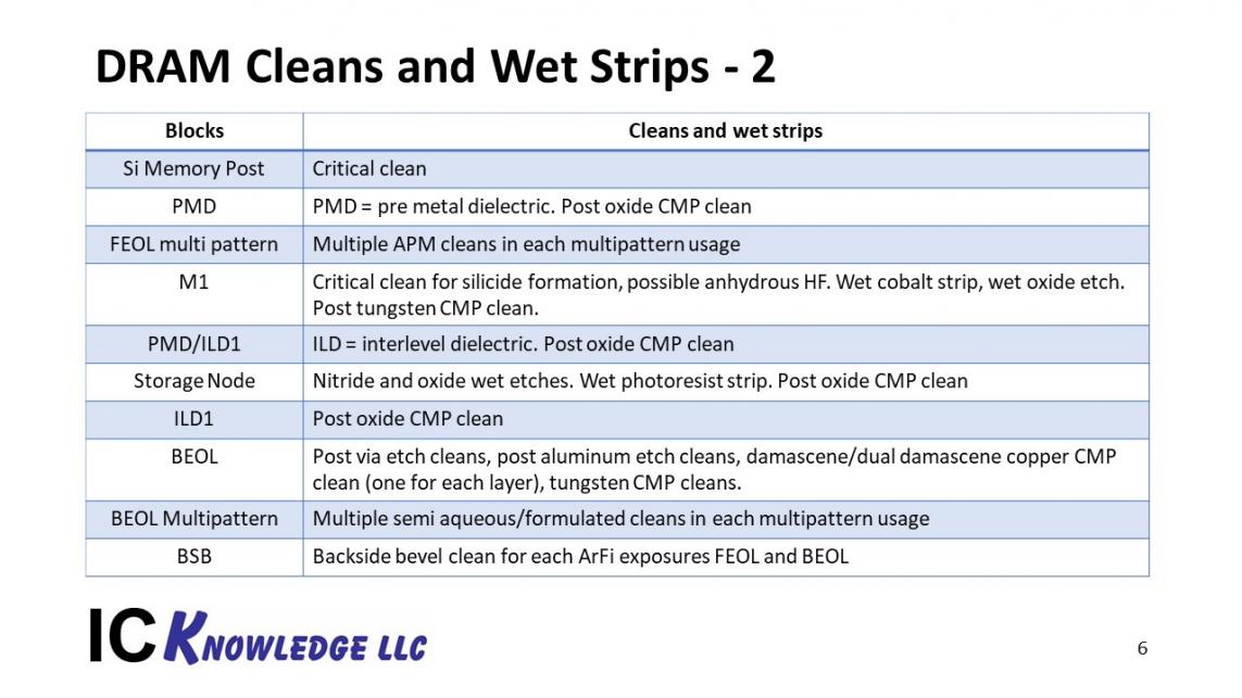
Presentation slide 6. DRAM Cleans and Wet Strips – 2
Slide 7 is my last DRAM slide and presents the number of cleans by node based on Samsung. Increasing DRAM clean counts are primarily driven by more backside bevel cleans required after immersion lithography steps and cleans related to increasingly complex multi-patterning schemes.
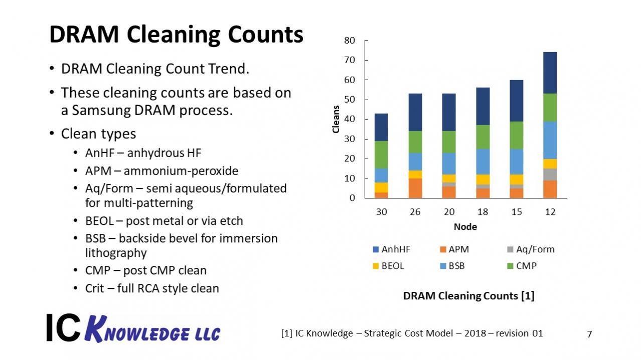
Presentation slide 7. DRAM Cleaning Counts
Logic
On slide 8 I present the logic nodes by year for GLOBALFOUNDRIES (GF), Intel, Samsung and TSMC. These are the four companies driving the leading-edge for logic. It should be noted that Intel’s node are generally equivalent to the next smaller foundry node, so for example Intel 10nm is similar to foundry 7nm.
See my leading-edge logic landscape 2018 article here for more information on logic nodes.
Underneath the table on the slide one the left side I show a cross section of a FinFET, the currently leading edge logic device of choice and on the right side I show a nanowire and nanosheet expected to begin to replace FinFETs around 4nm.
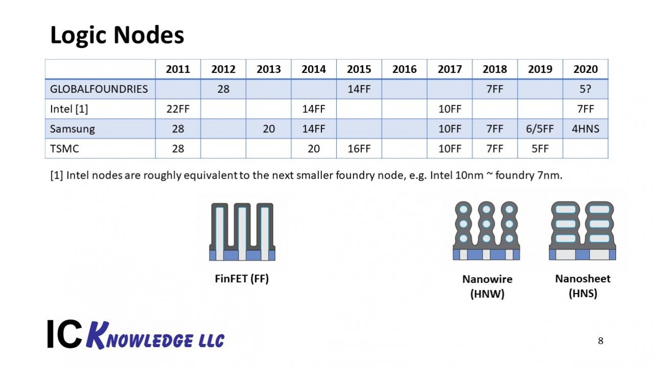
Presentation slide 8. Logic Nodes
In slide 9 I cover some of the major logic technology transitions. On this slide I show the intel/foundry nodes as two numbers representing the Intel node where the technology was introduced and the foundry node where the technology was introduced.
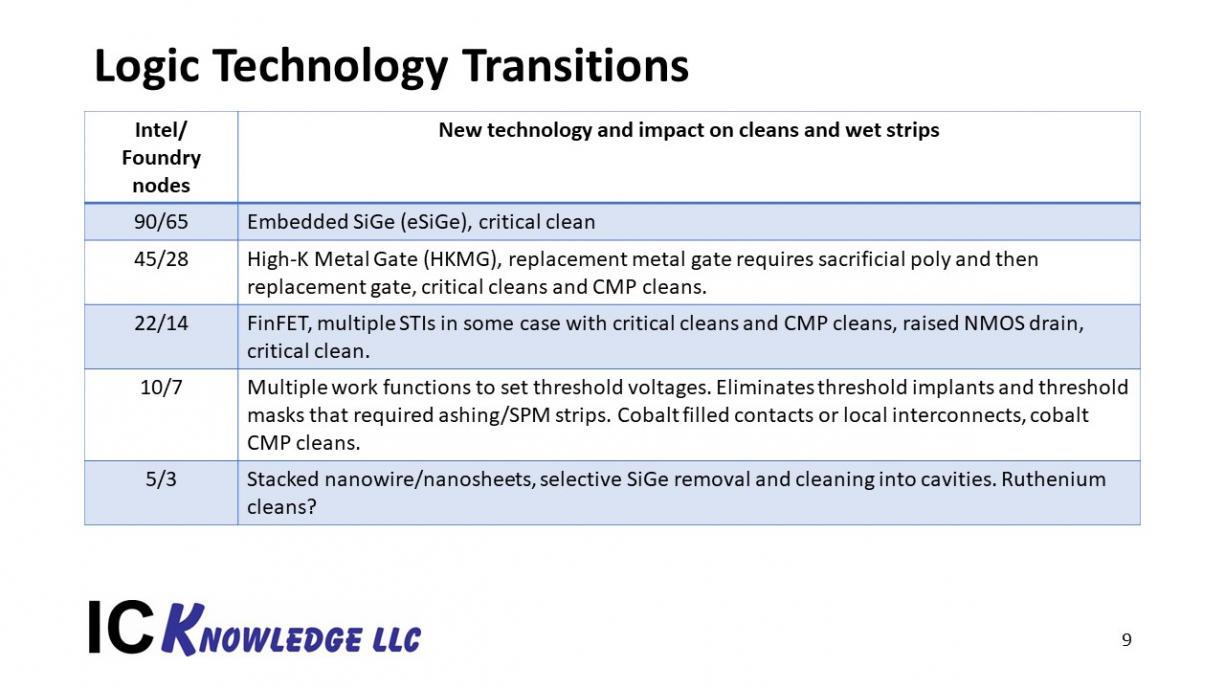
Presentation slide 9. Logic Technology Transitions
In slides 10 and 11 I go through some of the major Logic process blocks and discuss the clean and wet strip needs.
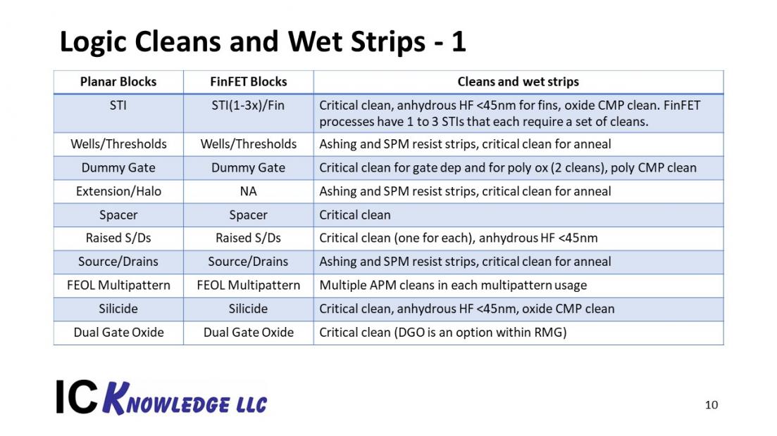
Presentation slide 10. Logic Cleans and Wet Strips – 1
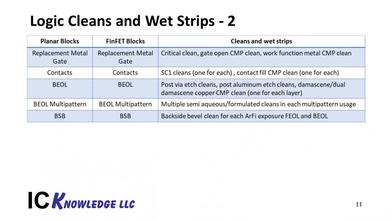
Presentation slide 11. Logic Cleans and Wet Strips – 2
Slide 12 is my final logic slide and presents the number of cleaning steps by node based on TSMC processes. The growth in logic clean counts is driven by increasing mask layers and multi-patterning complexity through the first 7nm optical node. Then at 7nm + and 5nm, EUV will significantly decreases the lithography complexity and eliminate many cleans.
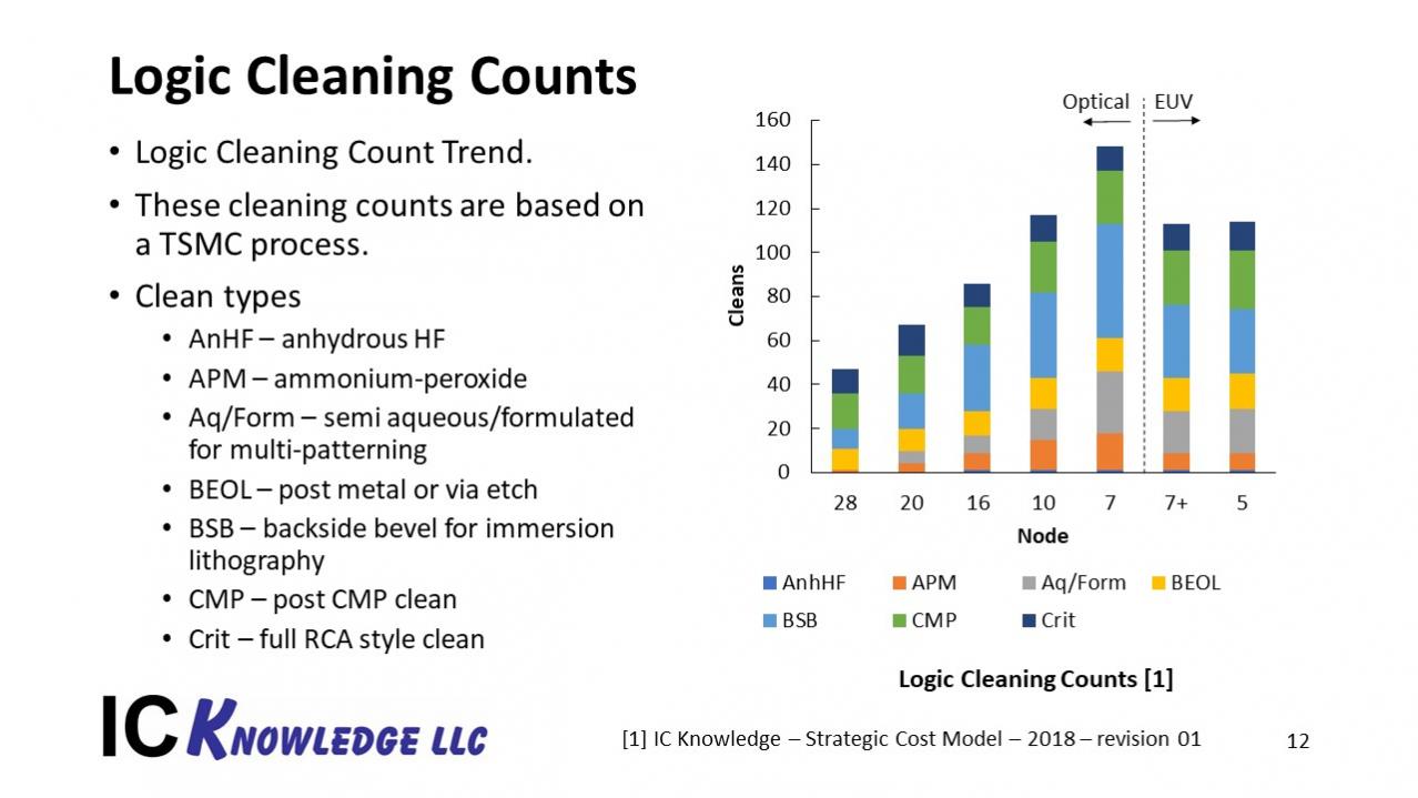
Presentation slide 12. Logic Cleaning Counts.
NAND
3D Has supplanted 2D NAND as the NAND technology of choice with 3D NAND bits now out shipping 2D NAND bits. 3D NAND scaling is layer based driven by deposition and etch in place of lithography driven processes such as were seen in 2D NAND.
In slide 13 I lay out the three main process segments for 3D NAND, CMOS fabrication, memory array fabrication and interconnect. The basic memory array process used by Samsung and Toshiba (the two biggest suppliers) is illustrated on the right side. As the number of layers grow eventually the memory array formation has to be split into multiple segment in “strings staking”, The figure on the bottom left illustrates the number of layers and strings for the three leading suppliers. Please note that the usage of string stacking is updated from the previous version of this slide presented at Nikon’s LithoVision and covered in my LithoVision write-up here.
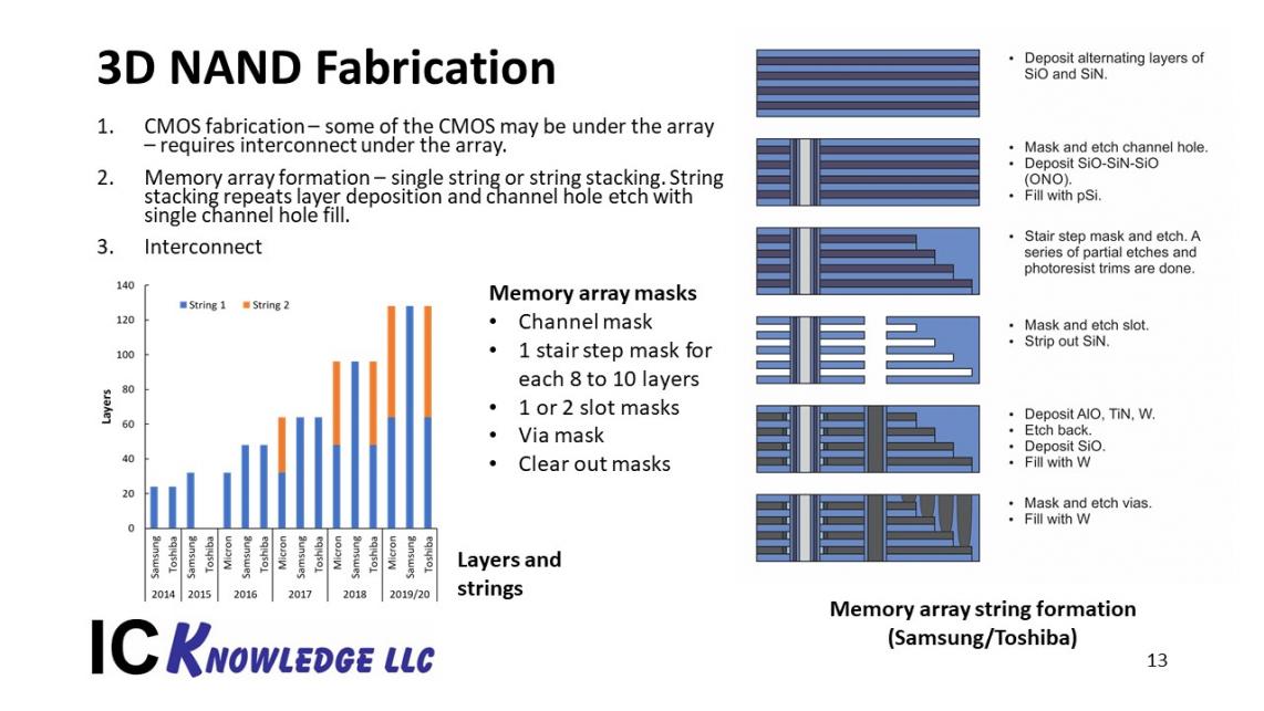
Presentation slide 13. 3D NAND Fabrication.
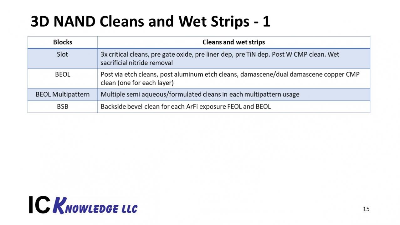
In slides 14 and 15 I go through some of the major #D NAND process blocks and discuss the clean and wet strip needs.
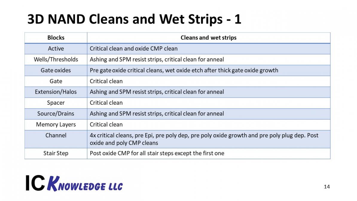
Presentation slide 14. 3D NAND Cleans and Wet Strips – 1
Presentation slide 15. 3D NAND Cleans and Wet Strips – 2
Slide 16 presents the total cleaning counts for 3D NAND versus number of layers for Samsung’s 3D NAND process. The big driver of additional cleans for 3D NAND is CMP cleans for stair step formation. After the first stair step mask each subsequent mask requires a sacrificial planarization layer with CMP before the mask is applied.
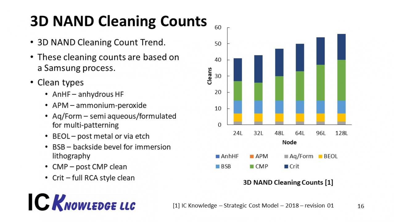
Presentation slide 16. 3D NAND Cleaning Counts.
Conclusion
DRAM scaling is facing fundamental physical limitations with no clear solution in sight. DRAM cleans are growing driven by lithographic requirements.
Logic continues to scale with 5nm and 3nm nodes on the horizon. Nanowires and nanosheets will present new cleaning challenges. Logic clean counts are growing driven by increasing mask counts and increasingly complex multi-patterning schemes.
NAND scaling has switched to 3D layers driven scaling. 3D NAND cleans are increasing driven by CMP cleans for stair step formation.
You can download the full slide deck here.
Share this post via:


Real men have fabs!