
At IEDM in December I had a chance to interview Thomas Ernst about the paper “Performance and Design Considerations for Gate-All-around Stacked-NanoWires FETs” by Leti and STMicroelectonics.
Leti published the first stacked nanowire in 2006, it was very new then, now stacked nanowire/nanosheets are starting to show up in commercial roadmaps. IBM working with Samsung and GLOBALFOUNDRIES has published on 5nm nanosheets at VLSIT in 2017 and Samsung has announced a foundry roadmap including 4nm nanosheets they refer to as multi bridge channel due in 2020.
Logic designs are built using standard cells where the size of a standard cell depends on the contacted poly pitch (CPP), minimum metal pitch (MMP) and track height, see figure 1.
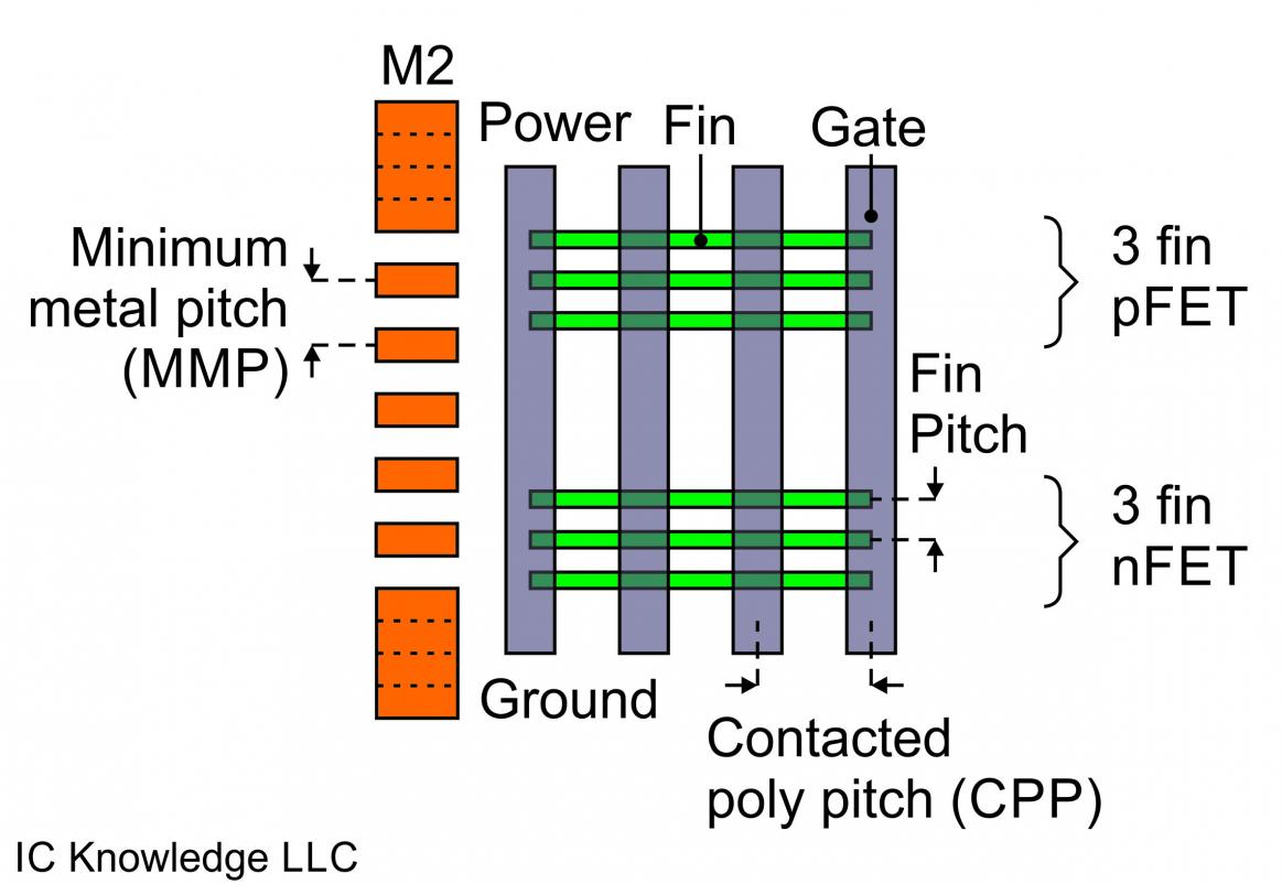
Figure 1. 7.5 track standard cell
In order to shrink standard cells, the industry has moved to design-technology-co-optimization (DTCO) where CPP, MMP and track height are all shrunk.
CPP is made up of three elements, gate length (L[SUB]G[/SUB]), spacer thickness (t[SUB]SP[/SUB]) and contact width (W[SUB]C[/SUB]), see figure 2.
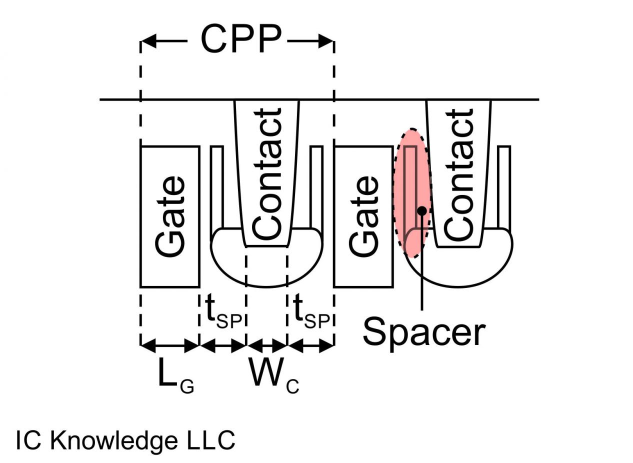
Figure 2. Elements that make up contacted poly pitch.
Where CPP is given by:
In order to maintain good electrostatic control, a FinFET with gates on 3 sides of the channel has a minimum L[SUB]G[/SUB] limit of around 16nm [1]. Gate-All-Around (GAA) adds a gate on the fourth side of the channel and improves electrostatic control enabling an L[SUB]G[/SUB] of approximately 13nm [1].
Another important consideration is how to achieve acceptable drive current at shrinking dimensions. Drive current is proportional to the effective channel width W[SUB]eff[/SUB]. One current trend in the industry is reducing track height that results in fin depopulation, for example a 7.5-track cell as shown in figure 1 has 3 fins for the nFET and 3 fins for the pFET, a 6-track cell as shown in figure 3, only has 2 fins for the nFET and 2 for the pFET. TSMC and GLOBALFOUNDRIES have both implement 6 track cells at 7nm. At the same fin height, the W[SUB]eff[/SUB] decreases as the number of fins is reduced.
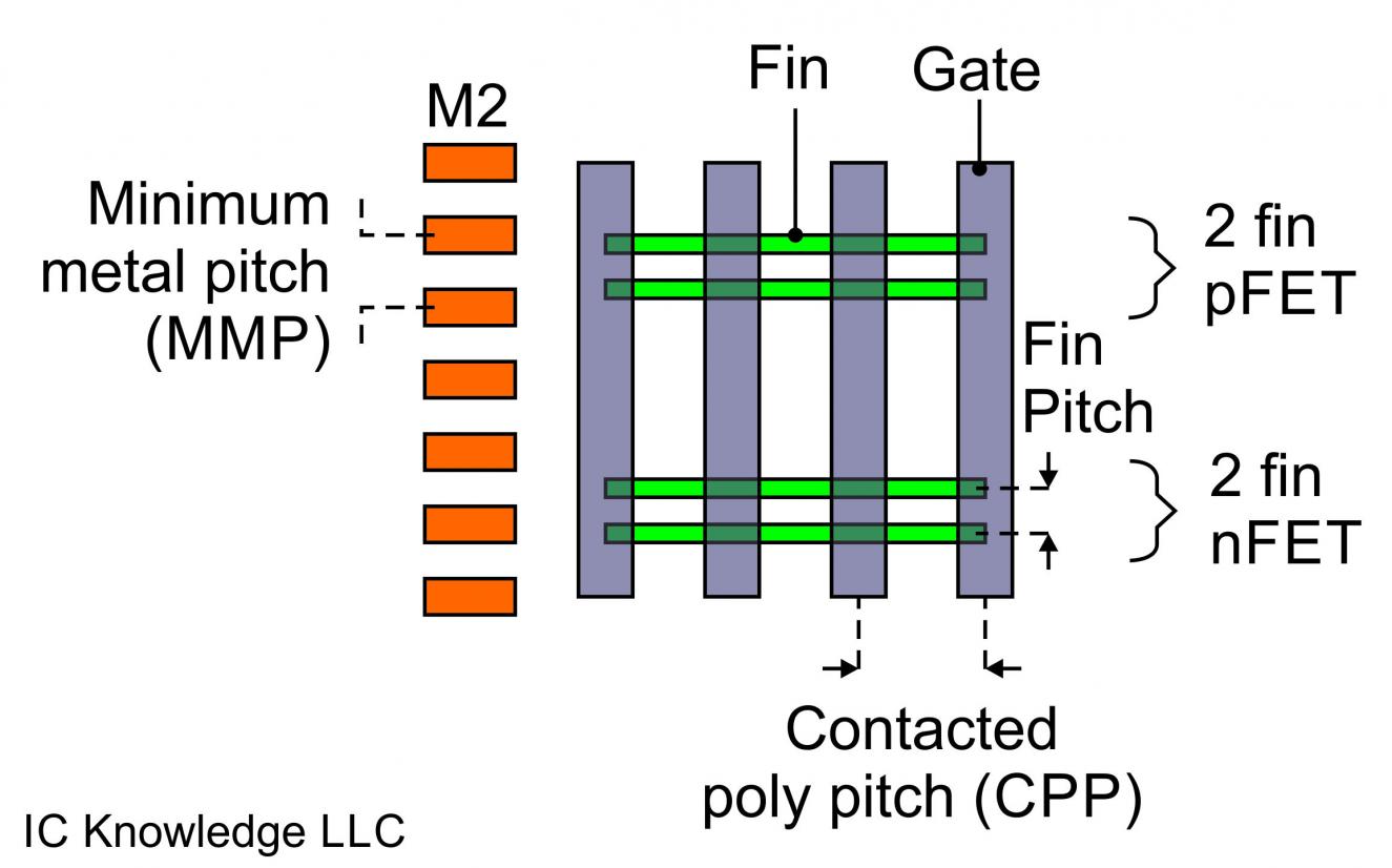
Figure 3. 6 track standard cell
Simply changing from a FinFET to a stacked horizontal nanowire with 3 wire and the same width and height as the fin, results in improved electrostatics but also a 14% reduction in W[SUB]eff[/SUB]. The ideal would be to be able to combine GAA electrostatics with FinFET drive current.
If instead of nanowires you make nanosheets by varying the width of the sheet you can achieve greater W[SUB]eff[/SUB] than a FinFET, see figure 4.
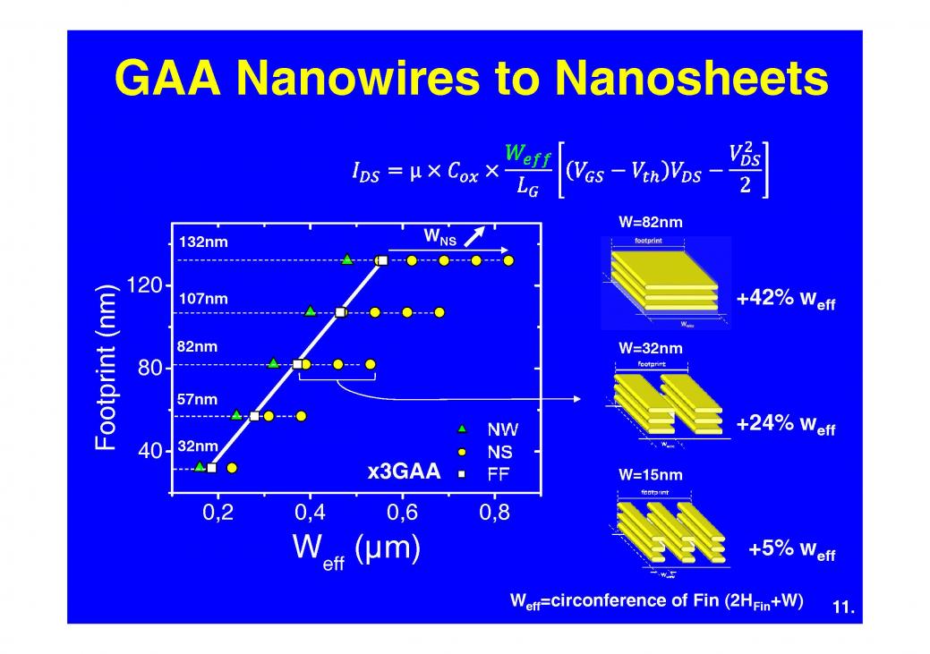
Figure 4. Weff for nanowires, FinFET and nanosheets [2].
The effect of nanosheet width on short channel effects is shown in figure 5.
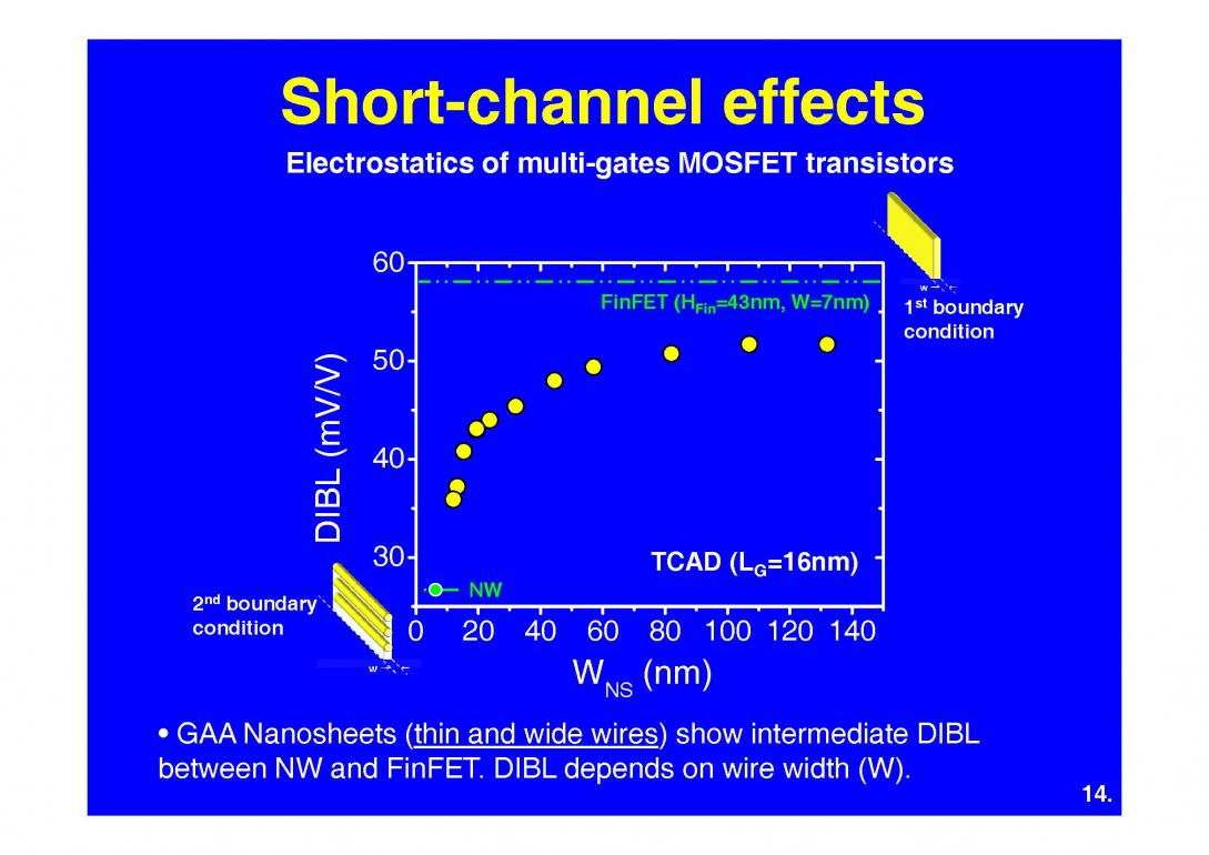
Figure 5. Short channel effects versus nanosheet width [2].
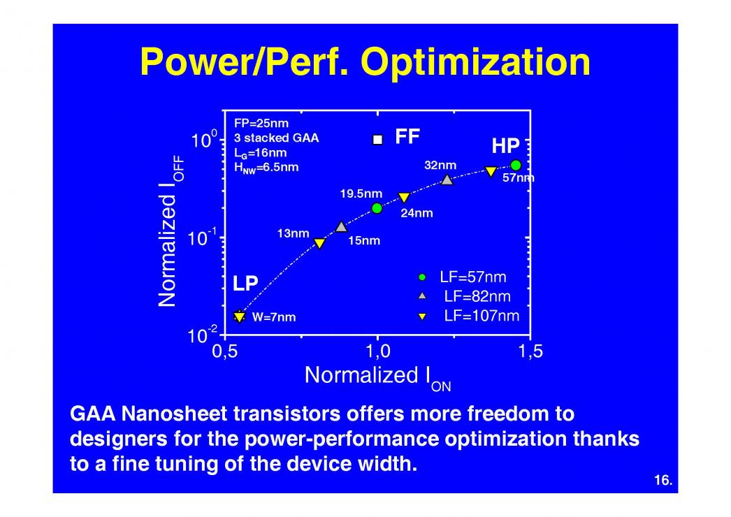
Between figure 4 and figure 5, you can see that nanosheets achieve better electrostatics and drive current than FinFETs. The ability to trade-off/tune drive current and electrostatics ultimately offers better overall power -performance and power-performance tuning than FinFETs, see figure 6.
Leti has shown patterning of up to 13 nanosheet layers while maintaining a crystalline film. There may be a trade-off between number of layers and performance due to capacitance, this is an area still being explored.
Strain management is critical to nanosheet performance and inner spacers are required to minimize capacitance.
There is still work to be done on nanosheet/nanowire development but it is showing great promise for post FinFET scaling.
In conclusion, horizontal nanosheets are a promising replacement for FinFETs with better electrostatics and higher drive current.
References
[1] J.P. Colinge, p 313, SISPAD (2014).
[2] S. Barraud, V. Lapras, B. Previtali, M.P. Samson, J. Lacord, S. Martinie, M.-A. Jaud, S. Athanasiou, F. Triozon, O. Rozeau, J.M. Hartmann, C. Vizioz, C. Comboroure, F. Andrieu, J.C. Barbé, M. Vinet, and T. Ernst, ” Performance and Design Considerations for Gate-All-Around Stacked-NanoWires FETs.” p 677, IEDM (2017).


Real men have fabs!