
At the IEDM 2017, imec held an imec technology forum and presented several papers, I also had the opportunity to interview Anda Mocuta director of technology solutions and enablement. In this article I will summarize the keys points of what I learned about the future of logic. I will follow this up with a later article covering memory.
Imec is one of the premier semiconductor research organizations in the world today and their work, and the papers and forums describing it, are always interesting.
An Steegen
An Steegen executive VP semiconductor technology and systems gave an overview presentation at the imec technology forum. Looking out five years some of the key developments by applications segment she expects are summarized in figure 1.
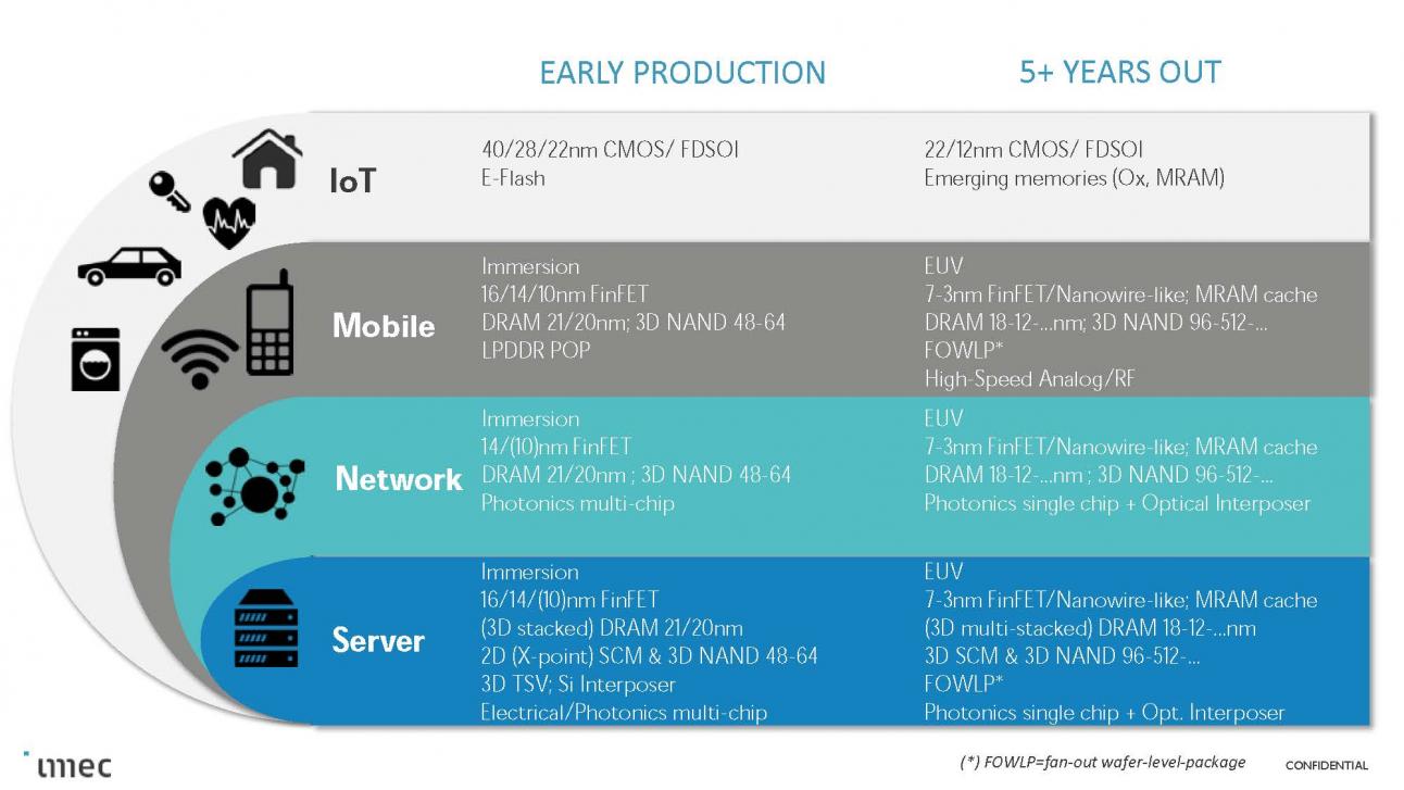
Figure 1. The next five years.
imec is doing a lot of work on nanowire/nanosheets and when and how to replace FinFETs and I will discuss that further below. Foundries will likely scale FinFETs to 5nm, beyond 5nm nanosheets appear to be emerging as the replacement technology of choice. Beyond nanosheets imec is looking at vertical FETs and complimentary FETs (n and p nanosheets stacked on top of each other). Vertical FETs look particularly attractive for SRAM.
imec is also putting a lot of effort into EUV, specifically photoresist and smoothing techniques for lower doses and lower absorption pellicles. I will be speaking about EUV at the ISS conference in January and I have been spending a lot of time looking at EUV readiness. Further improvements in pellicle transmission and low dose photoresist with acceptable LER are essential for successful EUV introduction to high volume production particularly for 5nm foundry logic processes.
Anda Mocuta
Anda Mocuta director of technology solutions and enablement followed An and focused on logic device scaling.
Traditional scaling provides a 50% area improvement for each new node. The foundries are having difficulty achieving a 50% area improvement just from contacted gate pitch (CGP what I call contacted poly pitch or CPP) and metal pitch (MP) scaling. Foundries have turned to track height scaling and design technology co-optimization (DTCO) as another scaling option. Figure 2 illustrates this scaling trend.
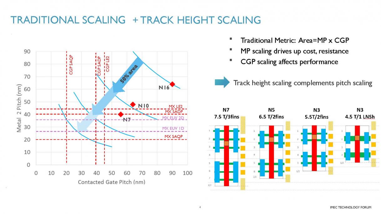
Figure 2. Scaling and track heights.
Authors note, both TSMC and GLOBALFOUNDRIES have 6 track cells at 7nm.
As you scale track height, fin depopulation is required with 4 fins for 9 track cells, 3 fins for 7.5 track cells, 2 fins for 6.5 to 5.5 track cells and eventually 1 fin for 4.5 track cells. Fewer fins mean less drive current unless other improvements are made such as taller fin heights. For 1 fin cells nanosheets become very important.
There are many scaling boosters that are being investigated:
- Self-aligned gate contacts – for example Intel has used this on their 10nm technology to enable contact over gate instead of contact over isolation as is typically done. Authors note, Intel claims this provides a 10% area improvement.
- Single diffusion breaks reduces the cell to cell spacing and width. Authors note, Has the potential to reduce cell width by 33% but in actual designs may be less.
- Super vias – vias connects interconnect layers to the layer directly above or below the current layer. Interconnect layer n is connected to n+1 or n-1. Supervias skip over the layers directly above or below to connect to n+2 or n-2. Authors note, TSMC has implemented supervias on their 10nm process.
- Buried power rails can “bury” the power rail in the substrate reducing the area taken up by interconnect.
I also interviewed Anda and she highlighted some key points from papers imec presented at IEDM.
Monte Carlo Benchmark of In0.53Ga0.47As- and Silicon-FinFETs
This paper looked at Ion/Ioff performance for InGaAs versus silicon. InGaAs has had a lot of interest as an alternative to silicon due to the much higher bulk electron mobility. In theory that should result in better performance.
What imec found is that when you consider contact resistance and traps the advantage is much less. Also at narrow fin widths confinement reduces on-current significantly. One of the big challenges is traps in the gate stack. Current state-of-the-art silicon is better but with gate stack optimization this could possibly be overcome. The bottom line is the window for InGaAs is small and closing as we move to smaller linewidths. Authors note, this conclusion is similar to work Morov presented at ISPSD in 2016.
Power Aware FinFET and Lateral Nanosheet FET Targeting for 3nm CMOS Technology
In this paper FinFETs were compared to nanosheets for a 3nm technology with a 42nm CPP, 21nm minimum metal pitch (MMP) and 21nm fin pitch (FP). The 21nm fin pitch was done with self-aligned-quadruple-patterning (SAQP) for both technologies and a 5.5 track height was used with 2 fins.
This new methodology is used to analyze devices performance versus devices type and parameters. Generally power requirements are harder to achieve than performance.
When scaling down to a 5nm technology, if you achieve a 40% power savings, a 35% speed increase comes for free. A further 5% power savings requires significant process complexity. Furthermore, as you scale below 5nm parasitics don’t scale well.
At 3nm you can still find a FinFET solution, but it requires high stress, low contact resistance, air gap spacers and other enhancements such as a SiGe PMOS channel. Every performance element is pushed to the extreme. Nanosheets can also meet the requirements at 3nm and under equivalent stress and doping can match FinFET performance and relax some parameters. Another interesting property of nanosheets is that by varying the width of the sheets density and performance can be traded off. This is easier to do within a design than varying fin heights.
26nm wide nanosheets with 2 sheets can provide sufficient drive current but needs high stress levels induced using strain relaxed buffers (SRB). There is some question as to whether the SRB stress will propagate all the way up the nanosheet stack. Nanosheets currently look very promising but there is a lot of work still to be done.
Stacked nanosheet fork architecture for SRAM design and device co-optimization toward 3nm
This paper presented a novel implementation of nanosheets where the gate is left off of one side providing space for more effective width. It is like turning a FinFET on its side and provides improved mismatch and power. Cutting the gate off one end does impact electrostatic control, with a few to ~15% reduction in Ion at the same Ioff but that can be more than offset by a wider sheet. Figure 3 illustrates the nanosheet fork versus standard nanosheets and FinFETs.
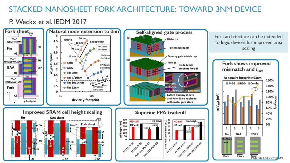
Ion and threshold mismatch are better than a FinFET or standard gate-all-around (GAA) at the same footprint and 2 nanosheets with a fork design can provide equivalent performance to 3 sheets in a standard GAA configuration. An SRAM in a fork sheet can be 20% smaller and have 2x the pull down of a standard GAA configuration.
Comprehensive study of Ga Activation in Si, SiGe and Ge with 5 × 10⁻¹⁰ Ω·cm2 Contact Resistivity Achieved on Ga doped Ge using Nanosecond Laser Activation
In this paper imec combined gallium and boron implants with laser annealing to lower PMOS contact resistance. Boron and Gallium each have their own activation and you can achieve more total active dopants than with either dopant alone. The net result is ~5E-10 contact resistivity and meets the requirements for 3nm. Contact resistance is a major parasitic element in leading edge technologies and is an area that has needed more attention.
Conclusion
The presentations from An Steegen and Anda Mocuta provide promising options to continue logic scaling beyond FinFETs well into the next decade.


Huawei’s and SMIC’s Requirement for 5nm Production: Improving Multipatterning Productivity