As I have discussed in previous blogs, IEDM is one of the premier conferences to learn about the latest developments in semiconductor technology.
On Wednesday December 6th, the Circuit and Device Interaction – Advanced Platform Technologies session was held, and Intel presented their 10nm technology and GLOBALFOUNDRIES (GF) presented their 7nm technology. Despite the different node names, the two processes have similar density. In this article I will combine previous disclosures, interviews and the papers to present a detailed comparison of these two leading edge technologies.
1.0 Processes
1.1 Intel 10nm
The key characteristics of the process are summarized as follows:
- Fins – The fins are patterned with SAQP and have a 34nm pitch, are 7nm wide and 46nm high. This is Intel’s third generation FinFET process. An interesting comment during the talk was that fin height can be optimized by product within an approximately 10nm range. The 46nm height quoted is slightly below the middle of the 10nm range.
- Gate – Contacted gate pitch (or Contacted Poly Pitch, CPP as I call it) is 54nm, presumably created with SADP. Dummy gates at cell boundaries are eliminated allowing neighboring cells to be isolated by a single gate width reducing area by 20%. Minimum gate length is 18nm.
- Spacers – 2nd generation low-k spacers reduce gate to contact capacitance by 7-8%.
- Source/Drain – In-situ doped raised source drains.
- Strain – 7th generation strain with in-situ doped raised source/drains and a novel NMOS strain orthogonal to the drain. The novel NMOS strain increases drive current by an additional 5%
- Work Function Metals – This is Intel’s fifth generation high-k metal gates (HKMG) (Intel introduced HKMG at 45nm ahead of the rest of the industry). All the threshold voltages for this technology are set by using different work function metals. The base process is 4 work function metals producing 2 threshold voltages, an optional 6 work function metal version provides 3 threshold voltages.
- Contacts – The process features cobalt filled contacts reducing contact line resistance by 60% versus tungsten and allows contacts over gate for an additional 10% density gains versus standard contacts over isolation. Contacts over gate are created using self-aligned gate contacts. Gate fill is recessed, a silicon carbide etch stop layers is deposited to prevent the gate contacts from shorting to the diffusion contacts and the contact fill is recessed (3 added steps). The self-aligned gate contacts are in addition to the diffusion contacts that were already self-aligned using a silicon nitride layer that was in the 14nm technology. The contact metal stack also includes a conformal titanium layer to wrap around the raised source/drains and a NiSi layer to lower PMOS contacts resistance. Contact resistance is reduced by 1.5x versus 14nm.
- Interconnect Layers– table 1 summarizes the interconnect layers. The process is described in the paper as having 12 interconnect layers but has 13 if you include M0 and both top metals in the table. The interlayer dielectrics are the same as the 14nm technology.
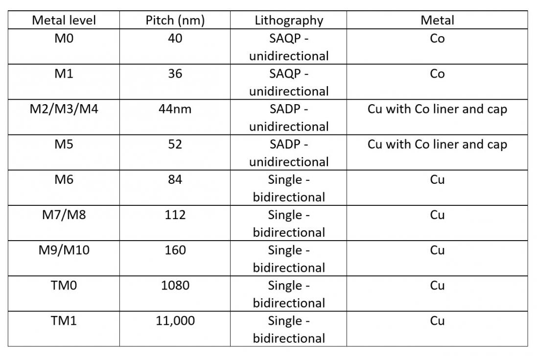
Table 1. Intel Interconnect stack.
- SRAM Cell size – High density SRAM cell size of 0.0312um2 and high-performance SRAM cell size is 0.0441um2. 0.56 volt VCC min for low power SRAM.
- Logic Cell Size – Minimum Metal Pitch (MMP) is 36nm with a 7.56 track cell for a cell height of 272nm. CPP is 54nm resulting in a cell size of 14,697nm2 (more on this later).
- Density – the process offers a 2.7x density increase over 14nm providing what Intel refers to as hyper scaling versus classic 2x density scaling.
- Ring oscillator – ring oscillators are 20% faster at the same leakage versus 14nm.
- TDDB – improved versus 14nm.
- EUV– Intel did not discuss EUV during this talk but did present a paper on EUV at the conference. Intel has 4 EUV tools that they are using for development and they have said they have an optical solution for their 7nm process but will use EUV if it is ready.
1.2 GF 7nm
The key characteristics of the technology are:
- Fins – The fins are patterned with SAQP and have a 30nm pitch. This is listed as GF’s third generation FinFET process, GF’s 14nm process was their first generation FinFETs, I am not sure what the second generation was, perhaps an enhanced 14nm version.
- Gate – Contacted gate pitch (or Contacted Poly Pitch, CPP as I call it) is 56nm, presumably created with SADP.
- Spacers – Not disclosed but I believe it is likely a 2nd generation low-k material such as SiOC.
- Source/Drain – raised source/drain epi is also optimized giving a 15% improvement.
- Strain – raised source/drains.
- Work Function Metals – 2nd generation using multiple work functions to set threshold voltages. GF used multiple work function metals on the 14nm FinFET process they run for IBM (14HP). 8 work function metals are used to provide 4 threshold voltages. All the threshold voltages for this technology are set by using different work function metals.
- Contacts – The process features cobalt filled contacts and trench implantation is used to optimize contacts for NMOS and PMOS. Optimization of implants and silicide gives a 39% benefit in contact resistance. Cobalt trench contacts reduce vertical resistance by 40% and when used for local interconnect reduce resistance by 80%.
- Interconnect Layers– table 2 summarizes the interconnect layers. The process is described in the paper as having 13 interconnect layers but has 14 if you include M0. The addition of cobalt liners and caps on M0 through M3 improves electromigration by 100x versus 14nm. Without this improvement 7nm power rails would be 3X wider than 14nm but they are actually 4x narrower. By choosing to limit the minimum metal pitch to 40nm SADP could be used. SADP allows wide and narrow metal lines on the same die versus more restrictive SAQP needed for <40nm pitches.
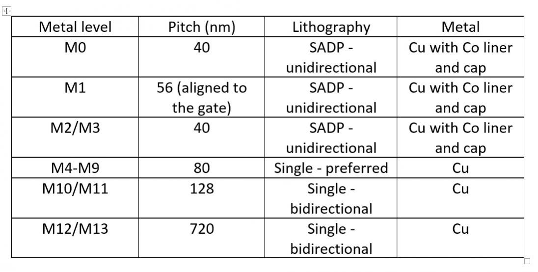
Table 2. GF interconnect stack. Details for stack A, stack B has additional pitch options and layers for M7 to M16.
- SRAM Cell size – High-density SRAM is 0.0269um2 and high-performance SRAM is 0.0353 um2. Write operations down to 0.5 volts for low power SRAM.
- Logic Cell Size – MMP is 40nm with a 6 track cell for a cell height of 240nm. CPP is 56nm resulting in a cell size of 13,440nm2. Larger 9-track cells are also offered for a 10% performance improvement.
- Density – the process offers a 2.8x density increase over 14nm and 0.36x scaling for common SOC blocks. GF spent a lot of time optimizing design rules to achieve this.
- Cost – Mobile 2 fin 6 track cell provides a >30% costs reduction versus 14nm and depending on the SRAM mix >45% cost reduction.
- MIM capacitor – the MIM capacitor offering is 2x the density of the 14nm MIM capacitor.
- ASIC – offering available as FX7.
- EUV– when EUV is ready a version of this process will be offered with EUV for contacts and vias. By limiting EUV to contacts and vias no shrink is provided but no redesign is required, and 15 masks collapses to 5 masks with a 1.5 day/mask saving in cycle time. One thing I find confusing about this statement is this implies 5 triple patterned optical mask layers becomes 5 single patterned EUV mask layers and yet during the talk 4 color contacts were mentioned. I suppose this could be something like 2 – quadruple patterned contact layers, 1 triple patterned via layer and 2 double patterned via layers. I asked GF to clarify this and they declined to provide that level of detail. A follow-on plus process is planned that will add EUV usage at metal layers providing a shrink but requiring a redesign. GF has been using the EUV tool at CNSE for development, in their Malta Fab 8, GF has 1 EUV tool being installed, 1 being delivered later in December and 2 due in 2018.
2.0 Discussion
In this section I will compare some of the key characteristics of the processes.
2.1 Fin shape
when Intel first introduced FinFETs at 22nm, the bottom of the fin was significantly wider than the top. At the time there was a lot written about the impact of this shape on performance. An ideal fin is rectangular with some rounding of the upper corners to prevent hot spots. If the width of the fin varies from top to bottom the different widths will result in different electrical behavior. I have heard that if you measured Intel’s early 22nm fins they actually looked like two transistors. Figure 1 compares Intel’s 10nm fin on the left to GF’s 7nm fin on the right. Fins are much more rectangular today than the were back in 2011 when Intel introduced their 22nm process. The GF process appears to have more rectangular fins than the Intel process.
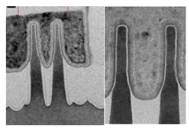
Figure 1. Intel fin shape (left) and GF fin shape (right).
2.2 Work Function metals for threshold adjust
Intel provides 4 or 6 work function metals for 2 or 3 threshold voltages and GF provides 8 work function metals for 4 threshold voltages. The number of threshold voltages likely represents the different process targets. GF is targeting foundry users that expect a high number of threshold voltages for low power applications and Intel is likely targeting high performance microprocessor applications. The use of work function metals to set threshold voltages allows the channels to be undoped, this provides two advantages. First, undoped channels have higher carrier mobility and therefore higher performance. Undoped channels also eliminate random dopant fluctuation (RDF) and make threshold voltage distributions tighter.
2.3 Cobalt versus copper interconnect
A lot has been made about Intel having cobalt and GF not having cobalt since these papers were presented. It has even been incorrectly reported that GF doesn’t have cobalt on their process. GF has cobalt filled contacts but doesn’t use cobalt for interconnect layers (although you can use the cobalt trench contact for local interconnect). Intel has cobalt filled contacts, 2 cobalt interconnect layers and 1 layer of cobalt filled vias.
The resistance of an interconnect line is illustrated in figure 2.
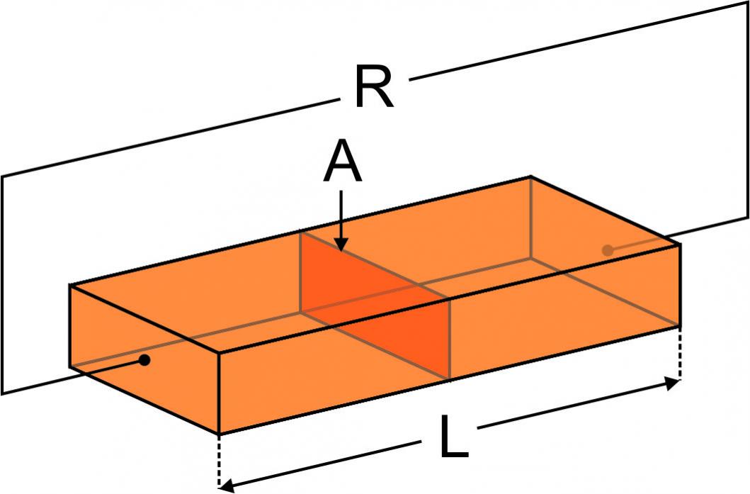
Figure 2. Interconnect line resistance.
The formula for resistance is presented in figure 3.
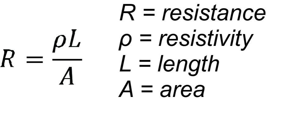
Figure 3. Formula for interconnect line resistance.
Copper replaced aluminum for interconnect use around the 130nm node because copper has a bulk resistivity of 1.664 microohm-cm and aluminum has a bulk resistivity of 2.733 microohm-cm. Cobalt has a bulk resistivity of 6.247 microohm-cm and you wouldn’t think that it would be an attractive candidate to replace copper in interconnect applications, however, at very small dimensions the resistivity of copper increases due to electron scattering. Cobalt is much less susceptible to this effect than copper due to an electron mean free path roughly one third of coppers. Also, copper requires thick high-resistivity barrier layers that don’t scale down in thickness and at small dimensions become a significant percentage of the cross-sectional area of the interconnect. Cobalt has more forgiving barrier requirements and the net result is that at a small enough linewidth cobalt becomes a lower resistance interconnect. The specific linewidth where cobalt becomes a lower resistance interconnect solution depends on several factors but is right around the linewidths being utilized here. My belief is that Intel used cobalt because they have a 36nm MMP and it made sense for them to do so. GF published a paper on 7nm process development with IBM and Samsung at IEDM in 2016 and that process had 36nm MMP and used cobalt for one level of interconnect. My belief is that with a 40nm MMP in the GF 7nm process cobalt wasn’t needed and it is more expensive than copper, so GF didn’t use it. Cobalt also offers higher electromigration resistance than copper and GF did use cobalt liners and caps around their copper lines to meet their electromigration goals.
The bottom line is Intel used cobalt because it makes sense for their process and GF didn’t because it didn’t make sense for their process. As we move to foundry 5nm and below processes I do expect to see more cobalt use and eventually ruthenium.
2.4 Density
When comparing process density there are many options in terms of metrics.
The size of a single transistor is the Fin Pitch (FP) multiplied by the Contacted Poly Pitch (CPP). The transistor sizes for the 2 processes are presented in table 3.
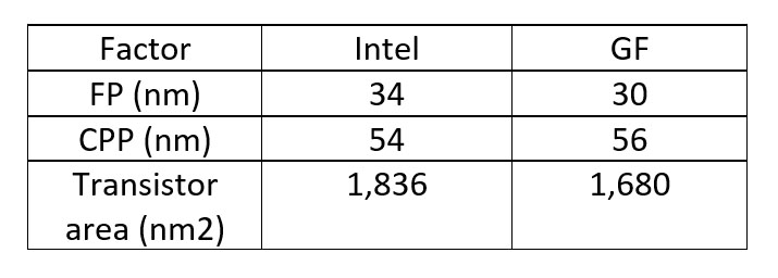
Table 3. Transistor size comparison.
By this metric GF’s aggressive FP leads to a smaller transistor size. The problem with transistor size as a metric is it doesn’t consider routing and isn’t reflective of actual design area.
Actual logic design is done using standard cells so metrics describing standard cell size are more useful. Figure 4 illustrates a 7.5 track cell similar to Intel’s 7.56 track cell.
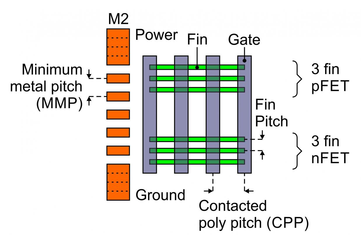
Figure 4. 7.5 track standard cell.
In process density comparisons from a few years ago it was common to use CPP x MMP as a cell size metric. Table 4 presents that calculation for the two processes.
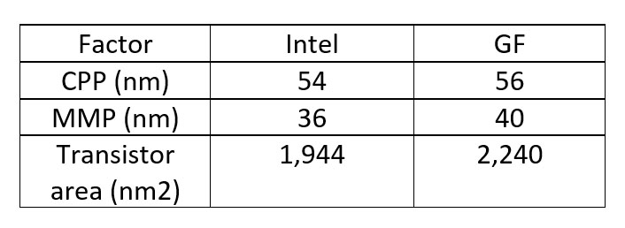
Table 4. CPP x MMP comparison.
By this metric Intel would appear to have the smallest cell size. The problem with this metric is that in recent years Design Technology Co-Optimization (DTCO) has become an important practice in technology development and track heights have become another scaling nob. From figure 4 we can see that the actual cell size is Track Height x MMP x CPP. Table 5 presents this data for both processes.
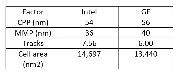
Table 5. Standard cell sizes.
By this metric GF has the smallest cell size. However, in the Intel section we discussed how Intel eliminated dummy gates at the cell edges and this enables tighter cell packaging.
Intel has recently tried to reintroduce a metric to the industry based on the area of a NAND cell weighted at 60% + the area of a scan flip flop weighted at 40%. Figure 5 presents the Intel method, this was also shown and discussed in the Intel paper.
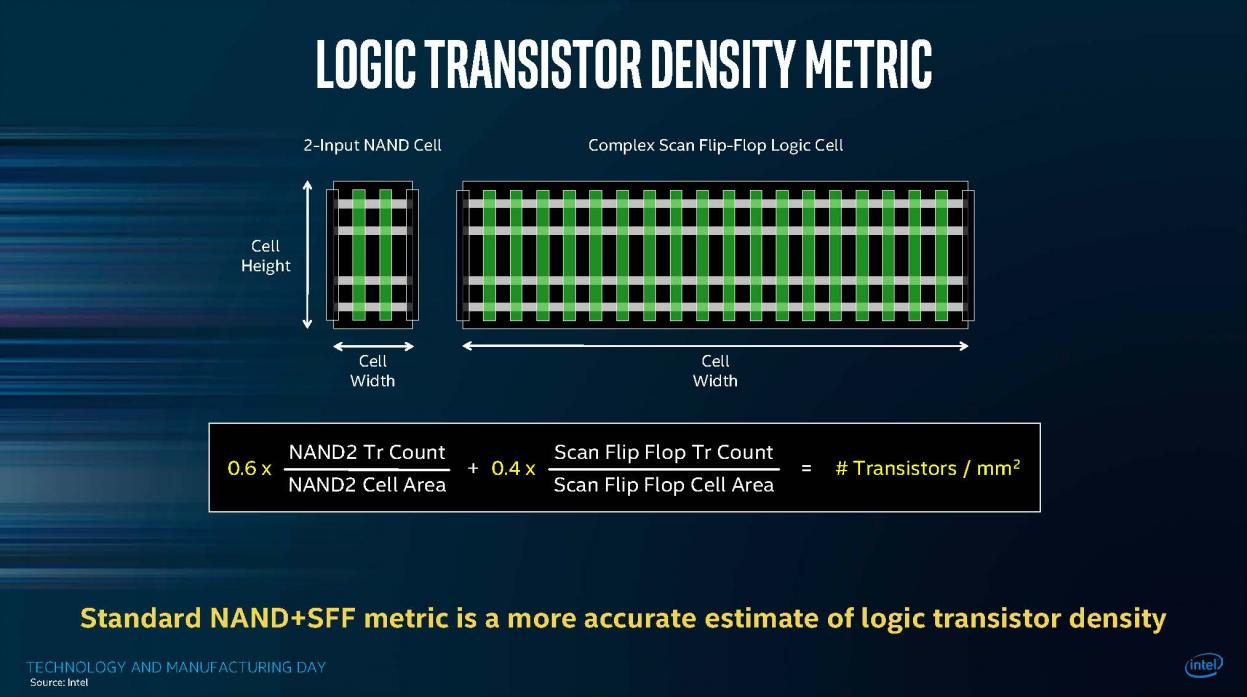
Figure 5. Intel density metric.
The claim is these cells and weightings are typical of logic designs. Intel has disclosed that by this metric their 7nm process archives 100.8 million transistors per millimeter squared. There are two problems with this metric, the first is Intel is the only company reporting based on this metric, the second is the foundries contend this metric doesn’t captures the subtleties of routing. In spite of these issues I have attempted to make my own estimates based on this. For Intel I get 103 million transistors per millimeter squared versus the 100.8 they report and for GF I get 90.5 million transistors per millimeter squared. The big difference here is that GF requires dummy gates at the edge of the cell and Intel doesn’t and that gives Intel a big advantage in the scan flip flop area.
High density SRAM cell size is 0.0269um2 for GF and 0.0312um2 for Intel so SRAM heavy designs will see an advantage with the GF process.
Ideally someone would design an ARM core in both processes and disclose how the size compares, baring that, after evaluating all of these metrics it appears these two processes offer similar density and the size of a design will depend on how the specifics of the design match up with the process characteristics.
2.5 Timing
The GF 7nm process is expected in the second half of 2018. The Intel 10nm is already late and I am hearing late 2018 and possibly even 2019 before it enters production. This presents a fascinating change in the semiconductor industry. Intel introduced 45nm, 32nm, 22nm and 14nm in 2007, 2009, 2011 and 2014 respectively. For many generations Intel was on a 2-year process introduction cadence, now they have gone to 3 years and 4+ years and while their scaling at 14nm was such that even at 3-years their yearly scaling pace was unchanged, they are now drifting off of that at 4+ year. It also begs the question of when Intel will introduce 7nm, are we now looking at 2022 or 2023?
In the mean time TSMC introduced 10nm in 2016/2017 and 7nm in 2017/2018 with 5nm due in 2019 and 3nm development underway. Samsung also introduced 10nm in 2017 with 8nm due 2017/2018, 7nm due 2018/2019, 6nm and 5nm due in 2019 and 4nm in 2020. GF is introducing 7nm in 2018 with a shrunk version due around 2019. GF hasn’t discussed 5nm yet but I would expect it this decade. With the foundry 7nm processes similar in density to Intel’s 10nm process and several foundry generations likely to come out by the time Intel introduces 7nm, I would expect a significant density advantage for the foundries over the next several years.
2.6 Performance
I wish I could offer a performance comparison between the processes but based on disclosures to-date I can’t. Intel is focused on microprocessor performance and GF and the other foundries are more focused on the mobile space and power for performance, beyond that I don’t have anything definitive to say on performance.
3.0 Conclusion
Comparing Intel’s 10nm process to GF’s 7nm process they are more similar than they are different. Since both companies are solving the same difficult physics problems this is in some ways not surprising.
The surprising part in my opinion is that GF at 14nm stumbled so badly they had to license it from Samsung. Now they have an internally developed 7nm process that matches up well with Intel’s latest 10nm process.
It is also surprising to me to see how far Intel has fallen from the process lead they had. First with HKMG by several years, first with FinFet by several year, I suppose they are still first to do cobalt interconnect but in terms of process density the foundries have caught them and appear poised to take a substantial lead over the next several years.
With Intel offering foundry processes and GF, Samung and TSMC all offering leading edge processes the industry now has four viable leading edge process options.
Share this post via:


Comments
45 Replies to “IEDM 2017 – Intel Versus GLOBALFOUNDRIES at the Leading Edge”
You must register or log in to view/post comments.