
Chip designers are familiar with the additional physical design checking requirements that were incorporated into flows at advanced process nodes. With the introduction of optical correction and inverse lithography technology applied during mask data generation, and with the extension of a 193nm exposure source to finer resolution dimensions, the traditional design rule checking (DRC) step was augmented with EDA tools that analyzed layout data to assess the fidelity of the final wafer-level structures to the original design. These algorithms were incorporated into checking tools described as providing Design for Manufacturability (DFM) support. (Parenthetically, EDA tools have also been developed to actively modify layout design data to reduce the “critical areas” that could contribute to yield loss, known as Design for Yield (DFY) modifications.)
DFM analysis has become increasingly important in the printed circuit board (PCB) design domain, as well. The scope of DFM analysis is significantly different for PCB design than chip design — PCB manufacture involves both bare board fabrication/test and subsequent component assembly. As a result, the DFM analysis for PCB design is an intricate interaction between Design for Fabrication (DFF) and Design for Assembly (DFA) requirements.
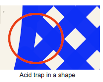
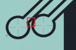
Examples of DFM checks for PCB design are illustrated below. The first depicts an “acid etch trap”, an area that may retain etchant longer than intended, resulting in open connections. The second figure highlights a design “sliver”, which is susceptible to detaching during the overall assembly flow, with the possibility of re-depositing and shorting distinct connections. Other examples include a trace routed through a solder mask opening created for a test point, or an analysis of the board stack-up thickness to via size aspect ratio to evaluate the drilling requirements and costs. These layout topologies are DRC clean, but represent additional risks during volume PCB manufacturing.

I recently had the opportunity to chat with Hemant Shah, Product Management Group Director for the Allegro PCB products at Cadence, about the expanding role of DFM for PCB design. Hemant impressed upon me the unique nature of this checking flow, as compared to IC design:
- PCB project development schedules are extremely aggressive
As a result, DFM analysis for PCB design needs to be an integral part of the design environment, with interactive results available for review.
- DFM analysis for PCBs requires access to the full board stack-up, layout, and component database.
Traditionally, multiple file formats have been used to represent the fabrication and assembly release data — e.g., Gerber drawings, CNC drill instructions, test specifications. The suite of DFM checks requires visibility into all PCB data, again necessitating integration with the design platform. (Hemant noted that the emerging IPC 2581 standard will be the comprehensive PCB release-to-manufacturing format for final analysis — please refer to www.IPC2581.com for more info.)
- PCB assembly introduces unique DFM analysis checks, beyond the IC realm.
The PCB Bill of Materials (BoM) is represented by a component library database, reflecting the schematic symbol, pad footprint, logical-to-physical correspondence, and 3D dimensional models. This library data is fundamental to DFA checking. For example, the automated optical inspection (AOI) head requires unobstructed visibility for (post-reflow) analysis of component placement/attach and detection of solder quality defects.
Hemant indicated that Cadence has addressed DFM analysis for PCBs with a new technology – the DesignTrue DFM – that is integrated into the Allegro Printed Circuit Design platform to provide real-time in-design DFM checks as the design is created.
“PCB layout designers routinely apply interactive DRC checking within Allegro. We have expanded that capability with DesignTrue DFM analysis, which incorporates over 2000 manufacturing rules. Layout designers can quickly get DFM results directly in Allegro, and evaluate them in the DRC Viewer.”, Hemant said.
Unlike the pass/fail nature of DRC rules, viewer support for DFM rules requires additional features. In addition to simply fixing DFM rule violations, layout designers can flag DFM results, assign a severity, and generate reports for broader review by the engineering team.
“How are these DFM rules developed, as part of design enablement?”, I asked.
Hemant replied, “The enablement team uses the familiar Allegro Constraints Manager interface to manage DFM rules. The rule values are commonly a combination of data from the PCB fabrication/OSAT and a customer-defined ruleset. Customers seeking multiple sourcing options may wish to establish their own encompassing rules. There is also the capability to define additional rules, beyond the 2000+ currently built into DesignTrue DFM.”
“Are DFM rules computationally expensive, especially for interactive checking?”, I inquired.
“There are seven different rule categories in DesignTrue DFM.”, Hemant indicated. Examples include: surface versus inner layer rules, rigid versus flex rules, stack-up and drill specifications, trace + via + soldermask + silkscreen rules,.
Hemant continued, “Layout designers can optimize their performance throughput by selecting specific checking tasks and/or restricting the analysis to specific regions.”
Design for Manufacturability analysis is no longer strictly part of the release handoff to the PCB fabricator, but has become a critical step in the PCB design phase. The interactive DRC checks in the PCB platform are expanding to include DFM checks, as well. The Cadence Allegro PCB DesignTrue DFM technology feature is indicative of this PCB design methodology trend — for more information on DesignTrue DFM, please follow this link.
-chipguy


Comments
There are no comments yet.
You must register or log in to view/post comments.