
Frequent Semiwiki readers are familiar with the importance of close collaboration between the foundries and EDA tool developers, to provide the crucial features required by new process nodes. Perhaps the best illustration of the significance of this collaboration is the technical evolution of layout parasitic extraction. All signoff-level electrical analysis flows rely upon an accurate (and where appropriate, concise) parasitic model. Increasingly, accurate and fast extraction algorithms need to be integrated with implementation flows to enable electrical optimizations during physical design.
The 7nm process node based on FinFET devices with local interconnect is emerging as a very attractive offering, with aggressively scaled circuit density, performance, and power over previous nodes — and, as with previous node transitions, the 7nm node introduces extensive requirements for both sign-off and integrated extraction.
I recently had the opportunity to chat with Hitendra Divecha, Product Management Director, and Hao Ji, Software Engineering Director, for the Digital and Signoff Group at Cadence. They described the numerous enhancements in Quantus QRC provided for the 7nm node. Here are but a few of the highlights of the new capabilities.
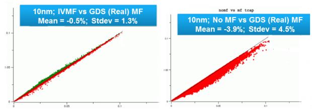
Integrated Virtual Metal Fill (IVMF)
Metal fill algorithm(s) are used to add metal shapes to the tapeout database, to provide improved data density uniformity (and density gradient uniformity) over a relatively small window area. The utilization of Chemical-Mechanical Polishing (CMP) for metal layer processing requires uniformity to prevent dishing profiles of interconnects after CMP.
The complexity of the (track-based and non-track based, multipatterning color-aware) metal fill patterns and design rules has grown with advanced nodes. And, the electrical (coupling capacitance) impact of the fill data to signals has also increased.
Yet, the signoff-level fill algorithms are too computationally expensive to be integrated in implementation flows — as physical design optimizations modify the routing data, the fill data needs to quickly adapt, as well. Cadence Quantus (and Innovus) have integrated a virtual metal fill and extraction capability. The IVMF algorithms optimize the fill cell size, and focus on accurate fill where the electrical model impact is greatest. The figure below depicts the high accuracy of the IVMF approach, relative to the final metal fill tapeout data.

Inductance Extraction
In previous process nodes, extracted inductive elements have typically been relegated to specialized tools that focus on the top metal redistribution layers of the power distribution network. The significance of inductive impedance is increasingly applicable to clock net distribution — this impedance strongly impacts the clock waveform characteristics from the clock source through repowering to the state point endpoints. Quantus QRC has incorporated Partial Element Equivalent Circuit (PEEC) algorithms to add inductive parasitics to the extracted model for clock simulation, used to provide more accurate clock arrival data for static timing analysis.
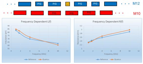
Specifically, there are algorithms to accurately identify the current loop(s) within the layout — a key requirement for any inductance calculation. And, the inductance extraction feature provides a model that is accurate across a wide frequency range — a key requirement to represent the impedance across the broad spectrum content of a high frequency, fast transition time clock signal.
Electromigration Analysis
Frequent Semiwiki readers are also aware that electromigration is an increasingly significant reliability concern at advanced process nodes, with two key issues.
- Self-Heating Effect (SHE)
The high areal current density and device channel profile of FinFET processes results in vastly different thermal energy dissipation than bulk FET processes. The temperature rise in the metal, contact, and via structures around active devices impacts both the resistivity and the metal migration activation probability associated with EM fails.
The Cadence Quantus and Voltus teams have collaborated with the foundries to develop an appropriate flow to integrate the SHE into electrical parasitic models for analysis.
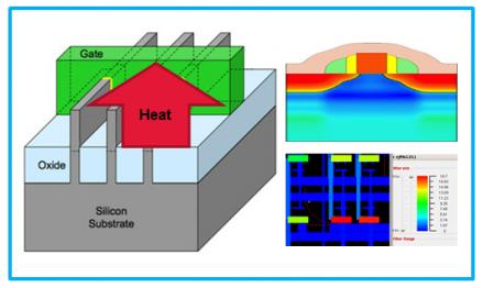
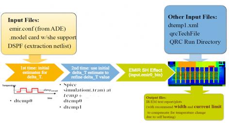
The figures above depict the thermal energy model and the (iterative) SHE calculation flow, with an initial delta_T estimate that is subsequently refined.
- Current Distribution Modeling
Another crucial facet to EM analysis is to develop a parasitic model that represents the detailed currents through each metal segment, contact, and via. There are some subtle nuances to this distribution that are prevalent in 7nm designs.
(1) pillar vias
The local currents of (high-drive strength) devices combined with the lithographic requirements of the 7nm node necessitate using multiple metal segments and vias to distribute the current — the figure below illustrates a “pillar via” consisting of a 2-by-2 array.
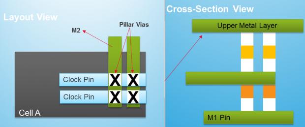
These pillar structures may use a simplified (reduced) model for timing and noise analysis, but require a detailed model for electromigration analysis to measure individual segment/via current distributions. Quantus has implemented algorithms for both modeling requirements.
(2) horizontal versus vertical currents (in local interconnects)
The use of local interconnects (often referred to as “M0”) in cell layouts in recent process nodes has resulted in substantial improvement in circuit density. The M0 layer(s) enables efficient connection across the source/drain nodes of fins in a device, local connectivity between different device gate/source/drain nodes, and an appropriate cross-section profile for subsequent contact to M1 metal segments.
As a result, the current flow in these segments is a combination of horizontal and vertical distribution, with different EM reliability limits. Quantus accurately models the M0 current directionality.
(3) logical versus physical pin detail
IP cell designs may offer multiple (or large area) logical pin shapes to enable a router to connect to the pin at any access point to minimize wiring congestion. Alternatively, the IP may add a “must connect” property to distinct physical pins to complete a single logical connection. The current distribution within the IP may be vastly different, depending upon how the connection is made. Quantus supports the extraction of a detailed view (in the presence of various logical pin designs and physical connectivity) that ensures the subsequent EM analysis utilizes an accurate current distribution.
This article has just touched on new extraction requirements for the 7nm process node. The biasing of layout data to meet lithographic requirements has become more complex, necessitating intricate correction factors within the Quantus QRC tool — this is magnified by the increasing application of multi-patterning decomposition and patterning.
For applications other than EM, parasitic model reduction is required to manage the size of the electrical model presented to other electrical analysis flows — the Quantus QRC team has also focused on reduction runtime for 7nm (without sacrificing accuracy).
The recent release of Quantus QRC to provide 7nm process node enablement is an excellent example of the collaborative design enablement with foundries. The new features address the additional complexities and requirements of advanced process nodes. For more information on Quantus QRC, please follow this link.
-chipguy
Share this post via:


Comments
There are no comments yet.
You must register or log in to view/post comments.