

I often read about the large number of expected IoT design starts around the world, so I started to think about what the barriers are for launching this industry in order to meet the projections. One of my favorite IoT devices is the Garmin Edge 820, a computer for cyclists that has sensors for speed, cadence, power, heart rate, altitude and temperature. The Edge 820 also communicates with Bluetooth and ANT+ wireless protocols, and has GPS to track each ride. At the recent ARM TechCon event there was a panel session on this topic of IoT design with participants from ARM, Mentor Graphics, Open-Silicon and Sondrel. This group came up with the following four barriers to using an SoC for IoT projects:
- Cost of the semiconductor IP blocks
- Cost of the EDA software tools for design and verification
- Silicon development costs
- SoC design experience
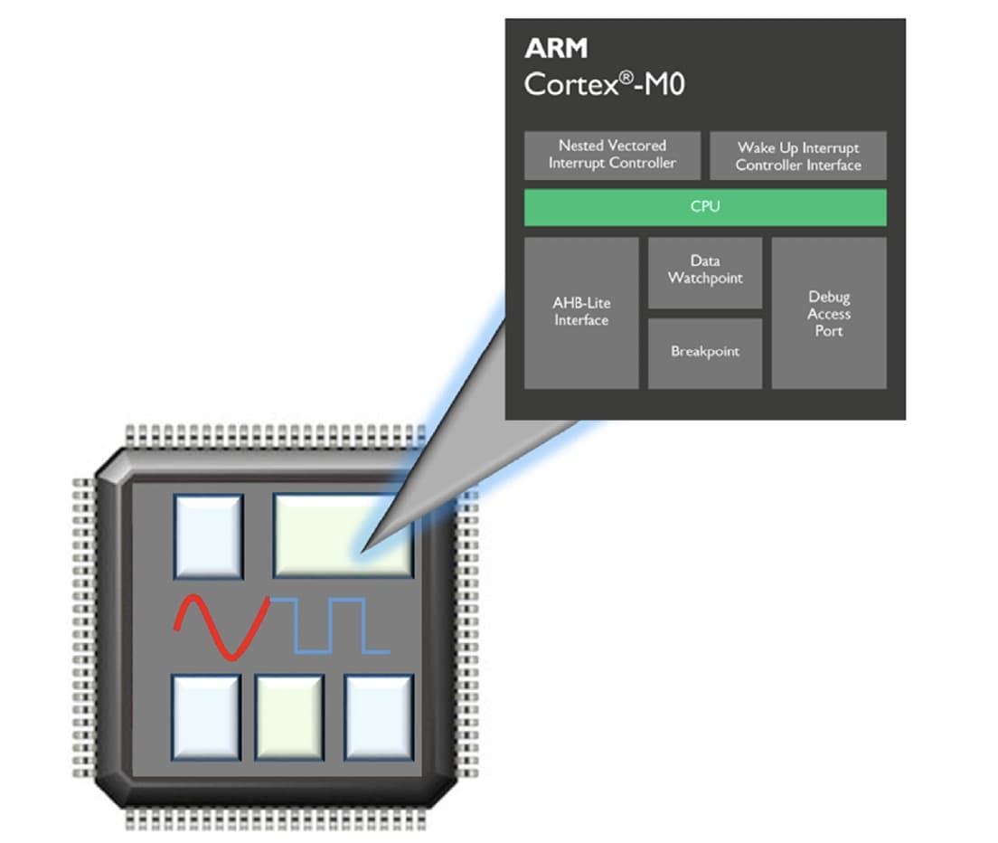
Typical IoT devices use sensors, which means processing analog signals, plus there is typically a processor to run an OS or code. Here’s a snapshot of the building blocks in most IoT chips:
NRE
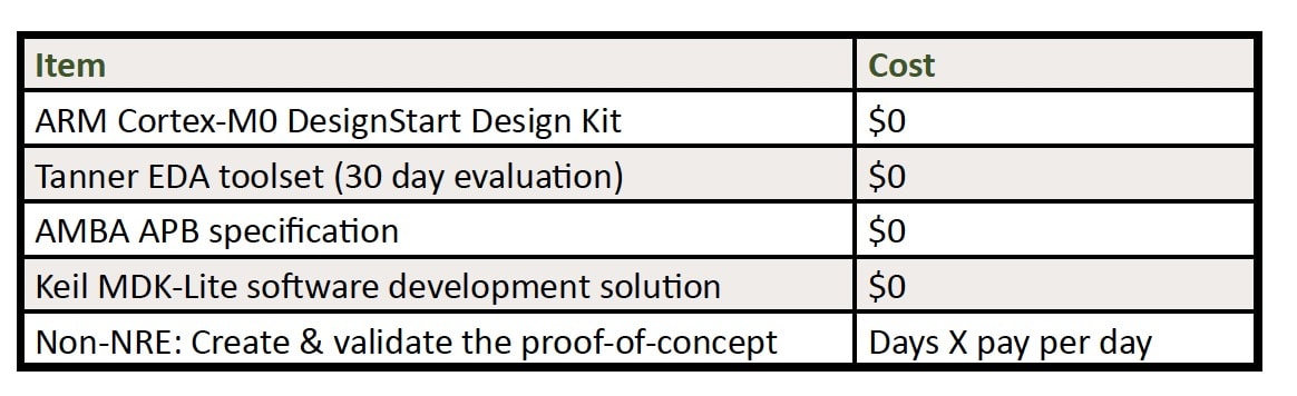
This acronym stands for Non-Recurring Engineering, and it appears in three of the top four barriers to creating an IoT project. So what if there was a way to reduce this NRE level so that you could do a proof of concept at little to no costs? Now that idea sounds compelling, and it turns out that ARM and Mentor Graphics have done something about it.
Related blog – Industrial IoT – Beyond Silicon Valley
ARM DesignStart
We’ve heard about the great success that ARM enjoys as an IP company offering CPU cores for many market segments, and they’ve created a way for designers t get a trial selection of their cores without charge, called DesignStart.
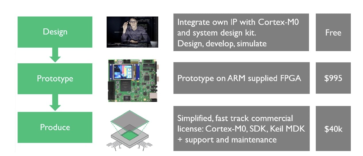
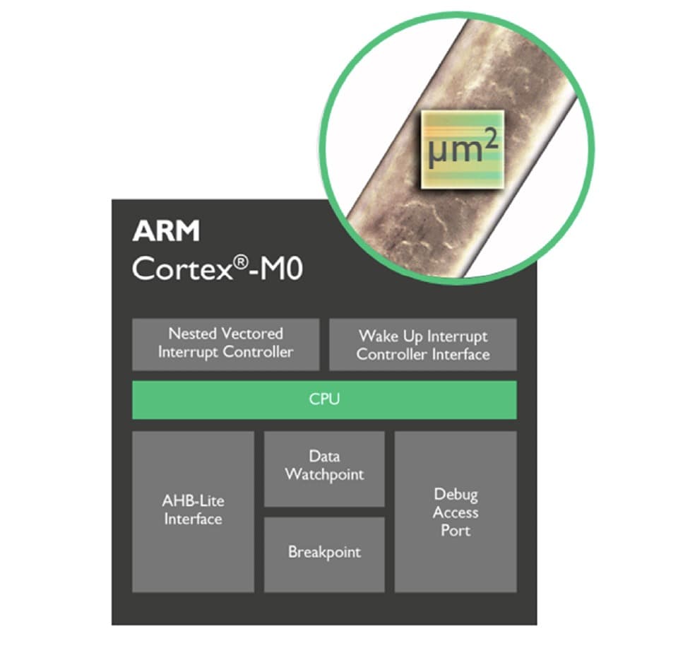
What DesignStart means is that you can get a free download and use for design and simulation their Cortex-M0. The M0 offers a low-power, 32-bit CPU in a very small size.
EDA Software Tools
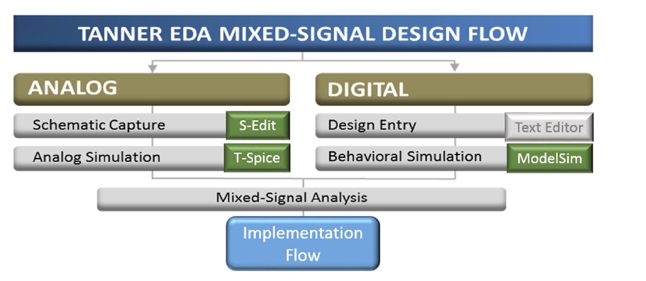
Now that you have a processor and some of your own analog IP blocks, you’ll need some EDA tools to do design exploration. There are free evaluation tools from Tanner EDA, part of Mentor Graphics, that last for 30 days, enough time to do a proof of concept. Design entry is done with schematic capture, and simulation is handled by T-spice for the analog portions and ModelSim for the digital blocks.
Related blog – IoT from SEMI Meeting: EDA, Image Sensors, MEMS
Sample IoT Design
To illustrate how you would use the ARM + Mentor design flow, consider an example IoT design with a sensor, ADC block, and Processor:
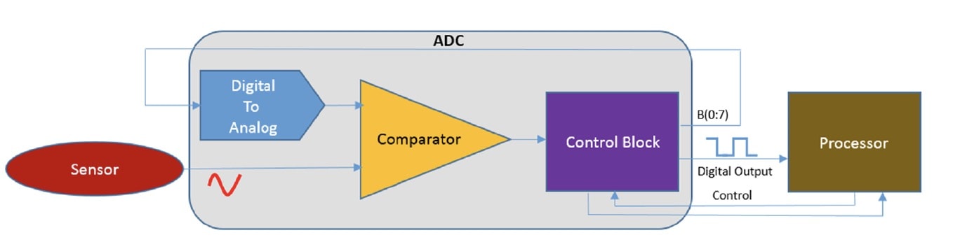
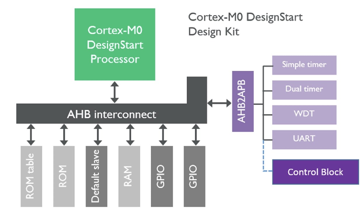
For this proof-of-concept design we’re just connecting up the components, but not running any code on the M0 processor, rather we are verifying the simple control logic between ADC and processor. In the Design Kit from ARM you’ll receive a pre-integrated processor subsystem with the following peripheral components:
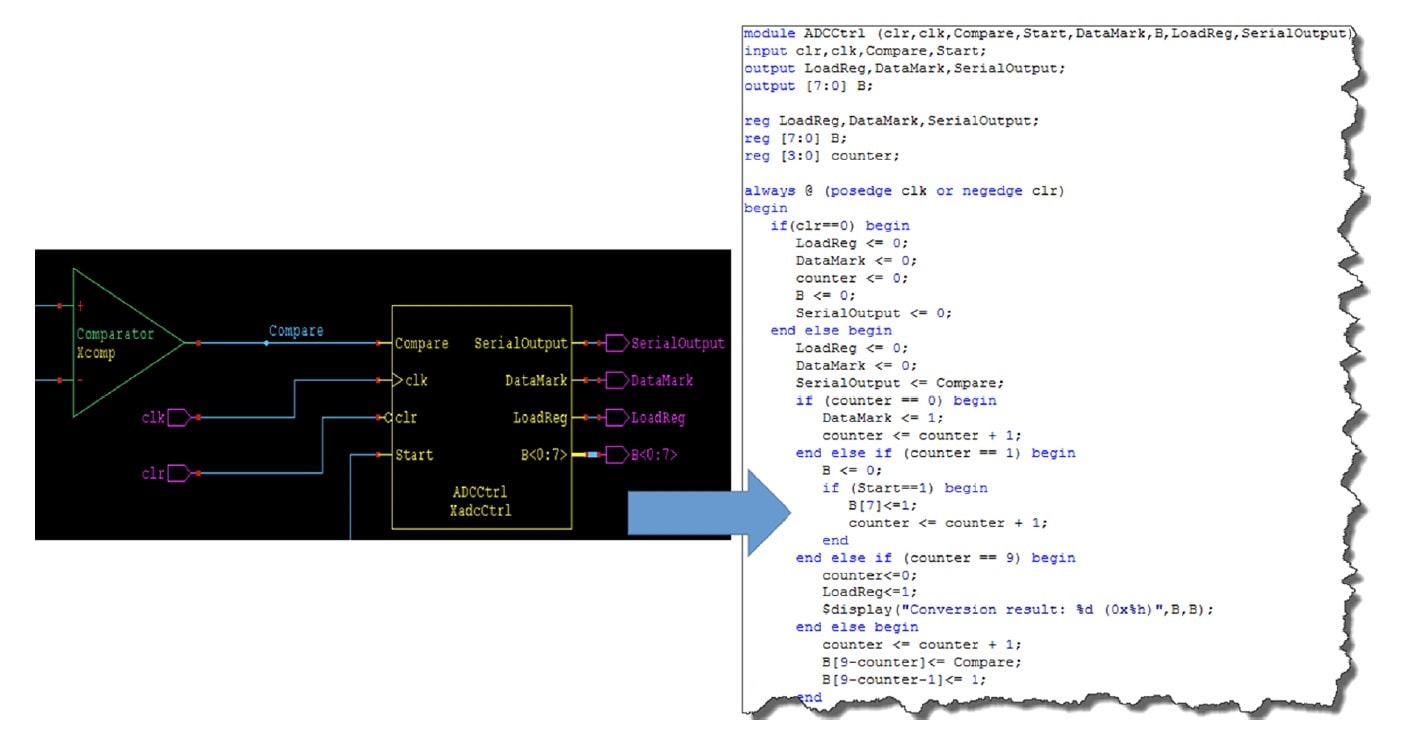
Our Control Block is shown in dark purple above so we next add Verilog code to describe the behavior using the text editor in S-Edit:
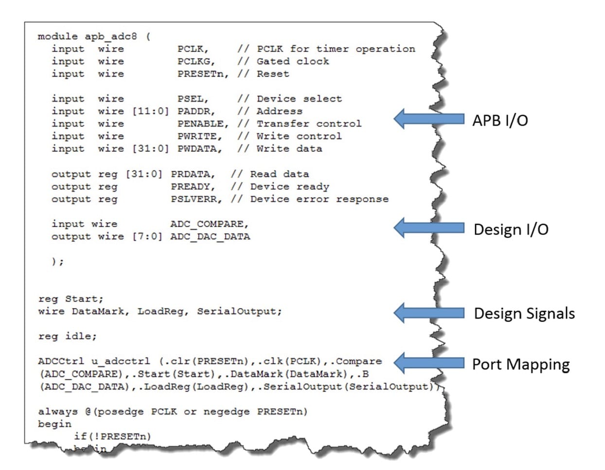
The control block connects to the subsystem bus, so we use Verilog again after learning a bit about the APB (AMBA Advanced Peripheral Bus) and create a module to define APB inputs and outputs, design IOs, design signals, and port mapping:
In Verilog we connect our peripheral to the M0, then we can write a simple text program for the M0 in C code using the ARM Keil MDK-Lite, a software development environment. Here’s the C code that sets the memory-mapped address of the APB port 15:
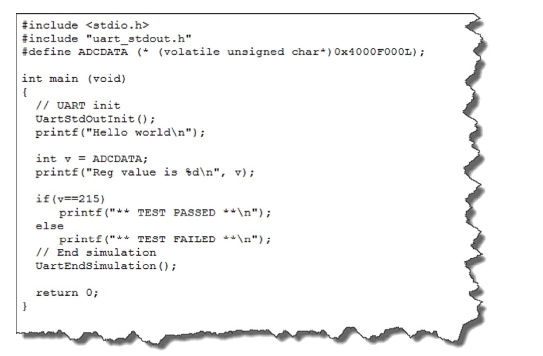
This C code runs printf statements in the simulator through the UART module. With an ADC input set at 1.8V and ADC reference at 2.2V, then we will expect an ADC output value of (1.85V/2.2V) * 256 = 215. If 215 counts were simulated the test passes, else it fails.
Simulating the IoT Design
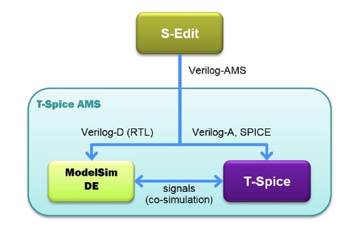
Design entry was done with S-Edit and the Verilog-AMS netlist gets split into two parts for simulation in either digital or analog simulators:
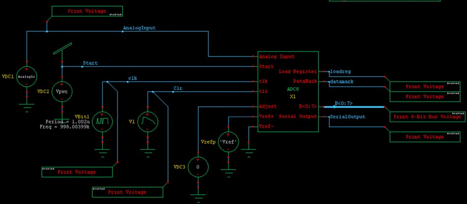
One last step is to create a design testbench that models the analog sensor input as a constant 1.8V, has a clock, and reads IO values for display:
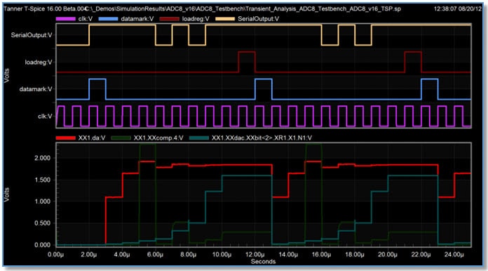
Our 8-bit ADC does a successive approximation that converts the analog input from the sensor into a digital value, read by the processor. In the waveforms below we can see the Red signal reaching the 1.8V level:
Summary
It is now possible to do a proof-of-concept SoC design for an IoT project at no cost, other than your engineering time by using processor IP from ARM and EDA tools from Tanner EDA. So the first three barriers listed at the start are now addressed, the fourth barrier is addressed by ARM where they have a list of SoC design partners to help you through the development process. There is an 11 page White Paper from Mentor with more details here online. I cannot wait to see all of the new IoT designs coming out over the next few years that will improve my life.


Comments
0 Replies to “Four Barriers to Using an SoC for IoT Projects”
You must register or log in to view/post comments.