

In the earliest days of IC design the engineering work was always done at the transistor-level, and then over time the abstraction level moved upward to gate-level, cell-level, RTL level, IP reuse, and high-level modeling abstractions. The higher levels of abstraction have allowed systems to be integrated into an SoC that can use billions of gates. All of that is wonderful and a powerful part that enables our global semiconductor economy, however if you are concerned about the quality and reliability of your SoC then keeping the Defects Per Million (DPM) very low is a key metric that must be adhered to. Having cell-aware diagnosis is essential to finding any manufacturing flaws at the transistor level, inside of standard cells, the basic building blocks of semiconductor IP libraries.
I connected with my contacts at Mentor Graphics to see what they are doing in this area of cell-aware diagnosis. Geir Eide has written a White Paper titled: Expose Transistor-Level Yield Limiters with Cell-Aware Diagnosis. I’ll share what I found it from this seven page document.
Like with any type of testing, you must first have a model of your standard cell library. In this case it starts with a transistor-level model that includes layout information plus the SPICE netlist. Many manufacturing defects occur based upon how the IC layout is arranged, just think about adjacent metal wires that potentially could short circuit. Taking a look at a diagram will help explain this new approach:
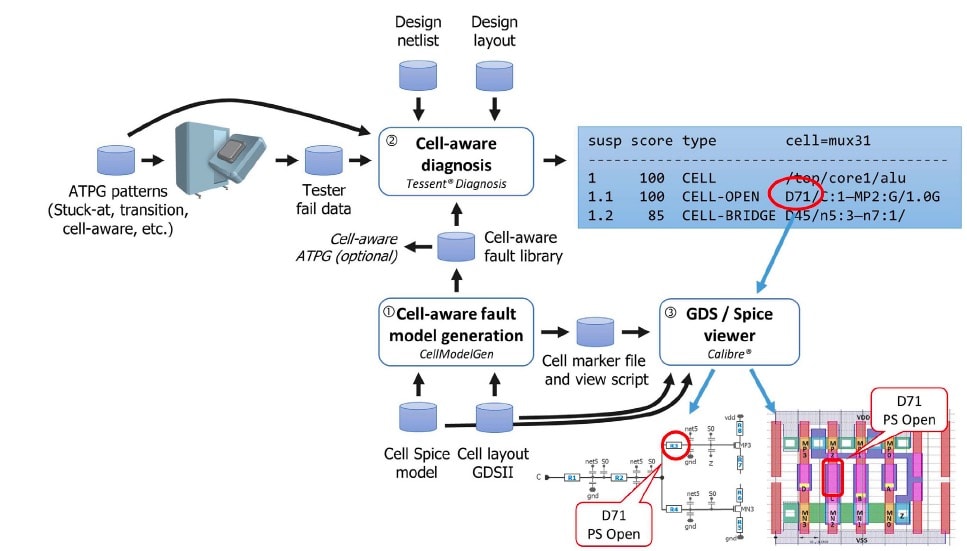
Starting at the bottom of the diagram we see that both a SPICE netlist and GDSII layout are inputs to the Cell-aware fault model generation step, this is where fault models are created by analog simulation for each of the potential defects extracted from the cell layout – think about shorts, opens and resistive shorts. In the diagram there’s an open circuit at node D71, which is inside of a particular standard cell. During the fault model generation a SPICE circuit simulator has predicted the behavior of having an open at node D71, so when we run our ATPG patterns then this particular fault can be detected, and during the diagnosis phase it will pinpoint the open circuit to be inside this cell instance at the specific XY coordinates. Think of how much time this approach will save your engineers that are performing Physical Failure Analysis (PFA) in order to improve the yield for a new SoC.
Related blog – New Frontiers in Scan Diagnosis
Product engineers are going to love this new ability, because it will make their jobs much more productive. So instead of just knowing that one cell instance has a defect somewhere, they now would now that inside of this cell instance at a specific coordinate, there is a defect, like an open or a short. Having this cell-aware diagnosis the yield problems can be quantified over a number of chips so that you can concentrate on PFA based upon the highest percentage issues found first.
Fault Model Creation
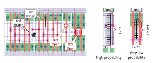
Now that we’ve seen kind of the big picture, let’s take a closer look at each of the steps starting with fault model creation. You create cell-aware fault models once per technology. During fault model generation the probability of an open or short between layers is determined, so for example in the following figure we know that bridging defect D45 has a high probability while defect D46 has a very low probability:
An analog simulator like Eldo is then used to simulate each of the potential defects against an exhaustive set of inputs to see if any input combination will produce an output result different from a good circuit. This data about which cell inputs can detect internal faults becomes part of the new fault model.
Diagnosis
During cell-aware diagnostics we see that the inputs are the SPICE netlist, layout, fault library, ATPG patterns and tester fail data:
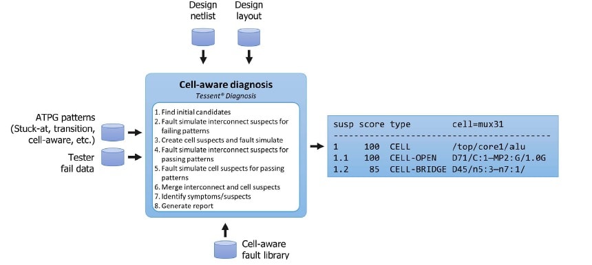
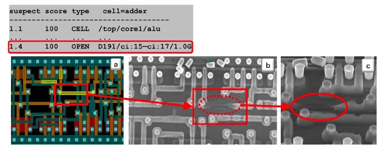
Every failing pattern is traced to find initial candidates using pattern matches. The best matching symptoms are identified and reported in the right-hand side. For me the biggest wow factor is the diagnostic ability to pinpoint the XY coordinates of each defect like opens and shorts between metals or poly layers. As you click on a text failure name, then you can see in the layout where this defect happened:
Silicon Results
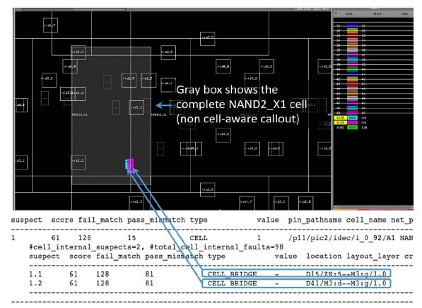
Up until now this all sounds so theoretical and practical, yet does it really correlate to actual silicon failure mechanisms in wafers? The short answer is Yes, according to a range of companies doing silicon designs from 160nm planar CMOS down to 14nm FinFET. One big name that uses this cell-aware diagnosis is AMD and here’s where they found an open contact defect inside of a full adder circuit:
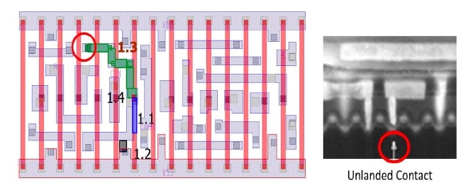
This one particular cell used 24 transistors and had 277 internal faults that could be tested based upon the extracted defects. In the old approach you would only know that this cell had a failure, while with the cell-aware approach now available you will know that four cell internal suspects would cause this particular failure. In the top-down view of the IC layout on the left we see all four of these suspects highlighted. The photo on the right shows a cross-sectional view of where the un-landed contact was pinpointed during failure analysis. You can quickly conclude that using this cell-aware approach is a great boon for PFA.
A second example shows how cell-aware analysis of a 160nm automotive chip pinpointed an open circuit on a Poly layer:
The IC layout is shown on the left in top view, then the middle is the silicon layout top view, finally the rightmost photo zooms into the missing Poly defect.
Conclusion
The goal of silicon manufacturing is to produce perfect chips, every time, however when there is a manufacturing flaw then the burden shifts to the product and yield engineers to quickly pinpoint the source of the failure in order to understand the root cause and propose a remedy or yield improvement approach. By using a cell-aware tool that models transistor-level defects inside of cells, the analysis work greatly speeds up, providing swift feedback about failures and yield. You could use this kind of a tool for both single-part diagnosis or yield analysis.
Read the complete 7 page White Paper here.


Comments
0 Replies to “Finding Transistor-level Defects Inside of Standard Cells”
You must register or log in to view/post comments.