

Did you know that, in over 800 teardowns of mobile and wearable products from 2012 to 2015, wireless chips outnumbered the actual number of products, indicating multiple wireless ICs in some designs ([SUP]1[/SUP])? It could be interesting to look at the advantages of integrating wireless technology such as Bluetooth low energy in a single SoC. Especially for systems where bill of material (BOM) cost and power consumption can be real issues, like Internet of Things (IoT) and wearable applications.
Bluetooth has been initially defined for short range usage, typically headset and smartphone, with paired device broadcasting approach. According with Bluetooth SIG, the future launch of Bluetooth 5 at the end of 2016, beginning of 2017, will suppress these limitations in term of range and broadcasting capability, and also double the speed and by consequence half the power consumption. Let’s have a look at the various wireless architectures integrating Bluetooth low energy, and the preferred process technology associated with each option.
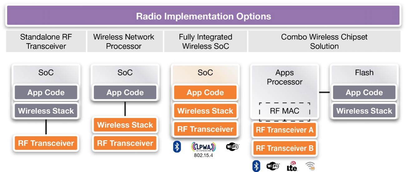
- Standalone RF transceiver: The controller and PHY are integrated in the transceiver chip that connects to the main SoC which houses the software stack and application code. RF transceiver is implemented in legacy nodes, like 180 nm.
- Wireless network processor: Several wireless protocols are integrated in a dedicated processor housing the wireless protocol stack, but the application code is in the application processor SoC. This network processor option target mature 90 nm node.
- Fully integrated wireless SoC: This monolithic, single die implementation is ideal for Bluetooth with the low energy technology for IoT applications. The Link Layer and PHY are integrated into the SoC that runs all software stacks and application codes. The 40nm and 55nm technology nodes are becoming popular for this monolithic option.
- Combo wireless chipset solution: Several wireless technologies such as WiFi and Bluetooth are integrated into a single transceiver connected to the SoC that includes the digital modem. All software, wireless stacks, and application codes reside in an external non-volatile memory. This solution is prevalent for mobile application processor and leverage aggressive process nodes like 28 nm, or below.
The combo wireless chipset architecture is offering unlimited off-chip memory, giving programmers more resources, but the number of chips (application processor + transceiver + flash) is too large if the goal is to develop a very low cost application, such as wearable or IoT device. Current wearable designs, like fitness wristbands, implementing Bluetooth LE for low bandwidth wireless connectivity, integrate only two chips: one SoC connected to a Bluetooth LE IC via a UART or I2C bus. It is now possible to push the integration for this type of application, by integrating the complete Bluetooth IP (Link Layer + PHY) into a single SoC. It’s technically possible, but what are the benefits?
A monolithic solution will offer the expected benefits like lower power, lower BOM cost and smaller footprint, all of these being extremely valuable for the target application. And it will also offer lower latency, as the data sent over the AMBA AHB bus can reduce latency by 5 to 10 cycles versus the SPI bus.
If we look more carefully at the power consumption, the two chip solution is made of a SoC, say in 40 nm or 55 nm, and one RF transceiver in 180 nm. Integrating the Bluetooth LE as an IP in the SoC will allow to seriously decreasing the power consumption part of the Bluetooth function. This function, implemented in a 180 nm process node (RF transceiver architecture), is now running in the SoC targeting 40 nm (55 nm) process node at much lower (Vdd) voltage, 0.9V for these ultra-low-power processes. This benefit is coming on top of the expected power saving going with the integration of two chips into a mono-chip. For battery powered devices like fitness wristbands, lower power consumption translate into longer usage, and the time between charges could make or break the product.
As mentioned earlier, the price point of a wearable or IoT device solution could be decisive. If it’s too high, the product will stay in a niche: cool, but too expensive to allow for wide market adoption. The wireless integration enables the removal of a complete chip sets, reducing packaging and test cost and removing duplication of power management. This can save over $0.15 in packaging costs and 20-30 extra pads that are required to support the additional wireless network processor. These savings, in conjunction with a reduced PCB footprint, make the total system cost savings very attractive.
The Bluetooth PHY is available on 180-nm, 55-nm and 40-nm process nodes allowing designers to also take advantage of the advanced processes’ power, area and performance benefits, especially on 55-nm and 40-nm. Moreover, the SoC development costs are still reasonable on these process nodes when compared with nodes below 28 nm. Unlike for very high volume applications like smartphone, or performance demanding like servers, targeting 55 nm or 40 nm process nodes allow enough power and cost savings to build successful systems for such low computing, low bandwidth systems.
Last but not least, the DesignWare Bluetooth Low Energy IP solution is qualified by the Bluetooth Special Interest Group (SIG) which is critical for designer success.
Eric Esteve from IPNEST
([SUP]1[/SUP]) According with a survey made by Teardown.com


Comments
There are no comments yet.
You must register or log in to view/post comments.