

 Low power is now a goal for most digital circuit designs. This is to reduce costs for packaging, cooling, and electricity; to increase battery life; and to improve performance without overheating. I talked to the experts on physical design for ultra-low power at Mentor Graphics recently about the challenges to P&R tools and the techniques used during design, particularly to control dynamic power consumption in FinFETs. Here’s what David Chinnery, R&D lead for low power, and Product Marketing Architect, Arvind Narayanan had to say.
Low-power design starts at the architectural level and continues through implementation. The challenge in implementation is to create, optimize, and verify the physical layout so that it meets the power budget along with traditional timing, performance, signal integrity (SI), and area goals. Physical design tools must find the best trade-offs when implementing a variety of low-power techniques. With the multiple layers of complexity in advanced technology node designs, power management requires a larger bag of tricks than ever.
Chinnery pointed out that low power as a design goal is nothing new. The basic low-power techniques, such as clock gating and use of multiple voltage thresholds (multi-Vt), are well-established and supported by existing tools. What’s new is the added complexity of meeting that goal at advanced process nodes and the increasing size and complexity of designs. There are a huge number of corner, mode, and power state scenarios that have conflicting requirements for power, timing, SI, manufacturability, and area. Additionally, with slower migration to new process technology nodes, there has been much greater emphasis on achieving the best possible design results using EDA tools with state-of-the-art low power techniques.
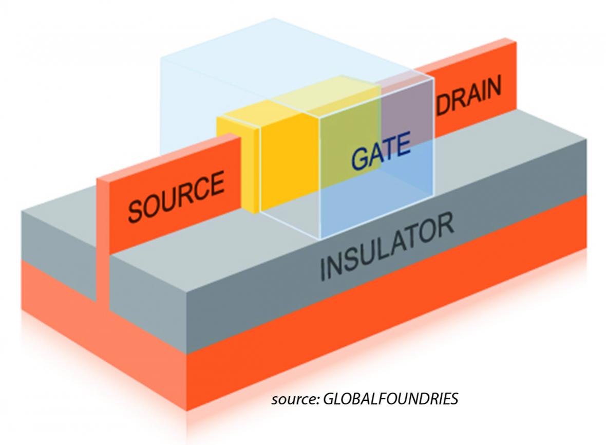 Narayanan added that FinFETs use significantly less total power, but the dynamic power component is much higher compared to the leakage power. The FinFET’s 3D gate around the transistor drain-source channel greatly reduces leakage due to better on/off control of the electric field in the channel. However, the 3D FinFET gate has higher capacitance compared to the MOSFET planar gate structure. Thus dynamic power needs to be considered during optimization and throughout the physical design flow.
So what can be done during physical design to control power?
Go in-depth with low power physical design solutions. Download the Mentor whitepaper, Low-Power Physical Design with the Mentor Place and Route System.
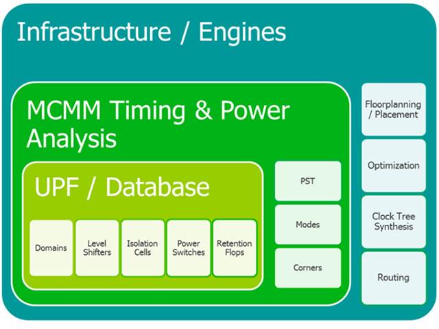
First, the tools must have the capacity to handle very large designs, 100+ million instances, with reasonable runtimes. Second, the tools must support the full bag of low power tricks. By “tricks” they mean techniques to reduce power like using multi-Vt, gate sizing, clock gating, multi-corner/multi-mode (MCMM) power optimization, pin swapping, register clumping, remapping, and power-density driven placement. But, Chinnery noted that designers also need full support for UPF 3.0 directives, multi-voltage flows, support for dynamic voltage and frequency scaling (DVFS) to handle varying supply voltages and clock frequencies, and the capability to handle special cells such as level shifters, isolation cells, and multi-threshold CMOS (MTCMOS) power gates. Deployed correctly, these advanced techniques and some additional secret-sauce optimization tricks result in power analysis reports that make everyone’s day a bit happier.
Chinnery and Narayanan agreed that one of the key strengths of Mentor’s physical design tools is the native MCMM architecture that lets designers analyze and optimize the design for all corner/mode/power state scenarios concurrently. Whether the design uses advanced process nodes and FinFETs or not, the MCMM capability is vital.
Also important for any low-power design, whether on a legacy node or the latest processes, is clock tree synthesis. Getting the best clock tree, said Narayanan, also depends on the ability to synthesize the clocks for multiple corners and modes concurrently in the presence of design and manufacturing variability, and in multi-voltage flows. He pointed to the importance of features like:
- Composing single-bit registers to multi-bit registers to reduce their load on the clock distribution network, and decomposing from multi-bit registers where necessary to meet data-path timing constraints
- Lowering leaf wire capacitance by register clumping and clock gate cloning/de-cloning
- Reducing functional skew and clock skew across multiple corners with MCMM CTS
- Useful skew to improve data-path timing and reduce power consumption
- Improving clock gating coverage with additional fine-grained gating
- Minimizing clock net switching power with smart clock gate placement to reduce wire length for high activity clock nets
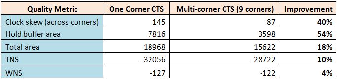
Using low-power CTS with MCMM optimization significantly reduces the number of buffers, skew, total negative slack (TNS) and worst negative slack (WNS), in addition to reducing dynamic power and area. The table shows some real customer data comparing a single-corner CTS implementation with a 9-corner CTS implementation for a single mode in a 9-corner design.
Another key part of the physical design flow is routing. For low-power designs, the router should follow the UPF power intent. This includes maintaining a single port of entry for boundary nets and respecting voltage island boundaries. The router handles secondary power connections for retention flip-flops, level shifters, and always-on buffers. Mentor’s router gets constant updates on MCMM timing and wire resistance and capacitance (RC), which it uses to find the optimal solution to meet power, timing, SI, manufacturability, and area constraints. It is also DFM-aware, so it accounts for the manufacturing issues that affect power (especially leakage power), such as variations in on-chip temperature and thickness.
For many IC designs, low-power is as important as timing. While you get the largest impact on power at the architectural level, Chinnery mentioned that a focus on low power throughout place and route can achieve a further 20% to 40% power reduction on some designs. Additionally, the place and route flow should remove the unpredictability from the physical implementation process that can result in late-stage surprises in power consumption. A blown power budget can affect the cost, performance, and time-to-market of low-power ICs.
For all the details on low-power physical implementation, download the Mentor whitepaper, Low-Power Physical Design with the Mentor Place and Route System.
Share this post via:


Comments
0 Replies to “Low power physical design in the age of FinFETs”
You must register or log in to view/post comments.