The recent announcement from Cadence, officially launching the PCI Express 3.0 Controller IP, as well as the associated Verification IP (VIP), made of Compliance Management System (CMS) which provides interactive, graphical analysis of coverage results, and PureSuite which provides the PCIe associated test cases, clearly demonstrate that the acquisition of Denali is bringing another fruit – after DDR4 Controller IP. Maybe some history will help. Back in 2006, Denali was known for their VIP products for Interface functions like PCIe, USB or SATA, when they first launch a PCI Express (gen-1 at that time) Controller IP. It was quite surprising, especially for their former partners, suddenly becoming their competitors! Nevertheless, they found a place on the market, positioning on the high end (and expensive) side, supporting Root Port or End Point and soon Single Root I/O Virtualization (SR-IOV), a solution targeting the PC Server market when Synopsys and PLDA where positioned on the mainstream PCIe IP market. Then PCIe 2.0 specification was issued, in 2007, and Denali was still in the race.
With the launch of this PCIe 3.0 solution, still in the emerging phase and probably reserved, for the moment, for high end, advanced applications, like storage, supercomputing, enterprise and networking, Cadence/Denali is following the same strategy: high end, high margin IP by opposite to mainstream solution, well covered by the competition. The customer mentioned by Cadence in their Press Release, PMC-Sierra, and the 6Gb/s SAS Tachyon protocol controller ASSP integrating this IP is clearly in this market segment.
Features
The PCIe core includes these features:
Single-Root I/O Virtualization
The PCIe core provides a Gen 3 16-lane architecture in full support of the latest Address Translation Service (ATS) specification, Single-Root I/O Virtualization (SR-IOV) specification, including Internal Error Reporting, ID Based Ordering, TLP Processing Hints (TPH), Optimized Buffer Flush/Fill (OBFF), Atomic Operations, Re-Sizable BAR, Extended TAG Enable, Dynamic Power Allocation (DPA, and Latency Tolerance Reporting (LTR). SR-IOV is an optional capability that can be used with PCIe 1.1, 2.0, and 3.0 configurations.
Dual-mode operation
Each instance of the core can be configured as an Endpoint (EP) or Root Complex (RC).
Power management
The core supports PCIe link power states L0, L0s and L1 with only the main power. With auxiliary power, it can support L2 and L3 states.
Interrupt support
The core supports all the three options for implementing interrupts in a PCIe device: Legacy, MSI and MSIx modes. In the Legacy mode, it communicates the assertion and de-assertion of interrupt conditions on the link using Assert and De-assert messages. In the MSI mode, the core signals interrupts by sending MSI messages upon the occurrence of interrupt conditions. In this mode, the core supports up to 32 interrupt vectors per function, with per-vector masking. Finally, in the MSI-X mode, the controller supports up to 2048 distinct interrupt vectors per function with per-vector masking.
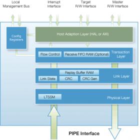
Credit Management
The core performs all the link-layer credit management functions defined in the PCIe specifications. All credit parameters are configurable.
Configurable Flow-Control Updates
The core allows flow control updates from its receive side to be scheduled in a flexible manner, thus enabling the user to make tradeoffs between credit update frequency and its bandwidth overhead. Configurable registers control the scheduling of flow-control update DLLPs.
Replay Buffer
The Controller IP incorporates fully configurable link-layer reply buffers for each link designed for low latency and area. The core can maintain replay state for a configurable number of outstanding packets.
Host Interface
The datapath on the host interface is configurable to be 32, 64, 128 or 256-bits. It may be AXI or Host Application Layer (HAL) interface.
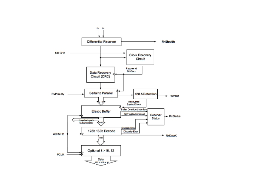
If we take a look more in depth into this PCIe gen-3 Controller, we see that Cadence has based the architecture on a 128 bit data path. This means, for 8 lane PCIe running at 8 GT/s, that the core is cadenced at 500 MHz (simply calculate 8 * 8000 / 128) which probably require to use technology nodes below 65 nm, as the core is –I guess- in the 500 K gates range, technology selection which is consistent with thesupercomputing and networking markets, and rather high end storage. Another remark we can do is that Cadence, as far as we can see, do not provide the PHY Interface for PCI Express function (PIPE). This version of the PIPE can run at 500 MHz for a 16 bit (or 250 MHz for a 32 bit and Cadence decided for the 16-b (per lane) Controller interface, allowing to keep in the same clock domain the PIPE and the Controller.
Apparently Cadence let the PHY IP supplier taking care of the PIPE 3.0 design, which makes sense as it may be necessary to position carefully the PIPE in respect with the PHY, in term of chip topology.
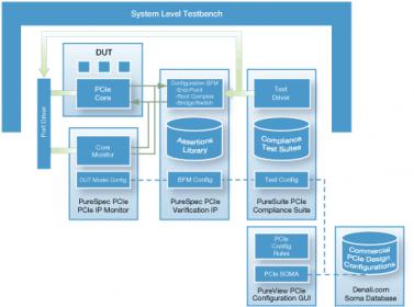
Offering the PCIe 3.0 VIP is a must, as Cadence is clearly and strongly positioned on Verification. If you consider the “size” of the PCIe 3.0 specification, counting more than 1000 pages, and offering many new features when compared with PCIe 2.0 and the latest engineering change notices (ECNs) such as ID-based Ordering, Re-Sizeable BARs, Atomic Operations, Transaction Processing Hints, Optimized Buffer Flush/Fill, Latency Tolerance Reporting and Dynamic Power Allocation, running Verification campaign on such an emerging product is a “must do”. Denali has always been very active in PCIe VIP, so Cadence has probably benefited from Denali’ long experience (seven years or so) for this protocol.
Eric Esteve


The Data Crisis is Unfolding – Are We Ready?