

The intricacies of analog IP circuit design have always required special consideration during physical layout. The need for optimum device and/or cell matching on critical circuit topologies necessitates unique layout styles. The complex lithographic design rules of current FinFET process nodes impose additional restrictions on device and interconnect implementation, and on device placement, which further complicates the analog IP layout task.
To manage some of the layout complexities, features have been added to the schematic/layout tools to record the design intent — i.e., a schematic database property (“constraint”) which can be used to assist with initial layout generation, and be checked against the final implementation. Yet, the need for additional analog IP layout automation remains a key issue.

I recently had the opportunity to review the topic of analog IP layout productivity with Bob Lefferts, Director of R&D for Mixed-Signal IP at Synopsys. Bob was passionate about the topic, and he should know — he manages the CAD team that supports over 1,000 analog IP designers and layout engineers, who deliver a breadth of IP functionality over multiple process nodes and multiple foundries.
First, a little background on analog layout design…
The implementation of analog circuits involves the judicious placement of devices — and especially, multiple device “fingers” — in a manner such that groups of devices will have matching characteristics. The goal is to reduce the sensitivity of circuit performance to mask overlay and fabrication on-chip variation, aka “OCV“. These same considerations apply to the interconnect patterns connecting matched devices (and their individual fingers).
To represent this design requirement, layout tools have been enhanced to accept constraints added to the design database. For example, schematic devices in a differential input pair can be tagged as “matched”; the corresponding device and pin layouts could have constraints added to require:
- a specific orientation (although most current FinFET process nodes require a single orientation for gates and lower-level metal layers)
- relative positioning
- min/max separation, or “bounding box” area limits
- alignment between devices (e.g., center/edge; horizontal or vertical alignment)
- symmetry of devices relative to an axis
A “centroid-type” layout of a diff pair has been used historically, as it reduces sensitivity to x, y, and rotational overlay tolerances.
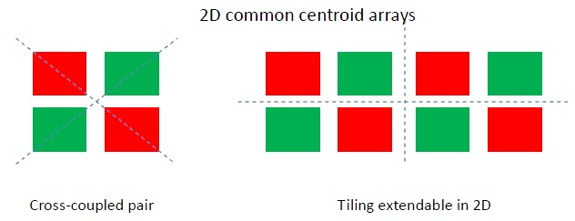
(Example of centroid orientations of multiple device fingers in a matched diff pair. )
A more sophisticated layout assist feature is to allow grouping of individual cells, such that all devices in the group are bound and move together.
Bob highlighted that these typical constraints are no longer sufficient in FinFET process nodes, due to additional requirements:
- minimizing local mask density variation
- assigning common multipatterning “mask color” layer designations, while simultaneously satisfying color density balance design rules
- incorporating dummy layout data for regular litho periodicity; satisfying FinFET-on-grid and gate periodicity restrictions
- matching layout-dependent effect (LDE) parameters in device models
An additional consideration that Bob stresses was the process design rule restrictions on device channel length and device channel width. His team is developing design flows in the most advanced FinFET process nodes, so that qualified IP is ready with production PDK releases from the foundries. These process nodes offer very limited options for device channel length, which severely hampers custom analog design. As a result, the implementation must incorporate multiple devices in series, to effectively realize a longer L value — this amplifies the complexity of generating analog layout to satisfy matching and variation-insensitive requirements.
Bob also spoke about constraint-driven layout, saying, “Several unsuccessful attempts have been made where EDA tools have asked the layout/design engineer to add textual constraints so the layout effort can be automated. But layout engineers don’t think like a programmer and instead operate in a visual context. Asking a layout person to create lines and lines of textual constraints is like asking an engineer to write poetry — only a very few will be successful.”
Bob clearly drove home the need for continued improvements in analog IP layout productivity, beyond the recording of constraints. He said, “We have a very close collaboration with the Synopsys custom tools R&D development team. Our design team meets regularly with R&D, and provides input on new features. These features invariably become part of the custom layout editor, schematic editor, and simulation environment. Specifically, we have worked on a unique method to improve the layout productivity on complex FinFET device and cell layouts. First, we place devices on interconnect tracks and then deal with fins, instead of snapping devices to fins, and then trying to make the interconnect line up. We also added a level of automation such that the layout engineer can concentrate on connecting devices to match the schematic while meeting all of the design rules.”
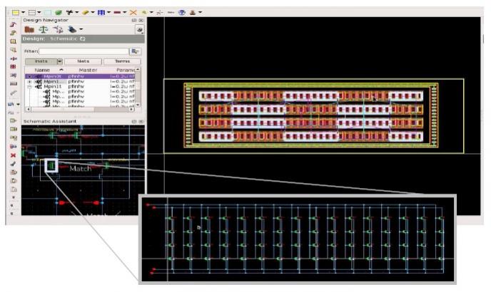
Complex pattern of matched series/parallel devices in analog layout (from Synopsys)
At the upcoming SNUG meeting in Santa Clara, Bob will be presenting details of the productivity gains that his design team has realized, and the results of the collaboration with the tools R&D team, in the talk “FinFET IP Design Using Synopsys Latest Innovation in Custom Tools” .
If you are a Synopsys user, I would encourage you to attend SNUG Silicon Valley on March 30-31, and Bob‘s presentation, in particular. Here are links to the SNUG registration and schedule:
https://www.synopsys.com/Community/SNUG/Silicon%20Valley/pages/default.aspx
-chipguy
Share this post via:


Comments
There are no comments yet.
You must register or log in to view/post comments.