

Albert Einsteinhad said, “In the middle of difficulty lies opportunity”. In today’s world dominated by technology, or I must say internet which has initiated collaborative information sharing, “leading from the middle” is the new mantra of life.
Similar situation is seen in the semiconductor ecosystem; it needs intense collaboration between different players in the overall value chain of semiconductor chip production. So there are tremendous opportunities in different forms to lead from the middle in the overall semiconductor ecosystem.
Mentor Graphics’ Calibre is a known golden standard physical verification solution to ensure designs are perfectly ready for manufacturing before getting into foundry. With this domain level leadership, Calibre is in a unique position among EDA tools, IP providers, Interfaces, and Foundries to ensure that the designs fulfil all criteria according to modern standards and within the specified parameters of a particular technology node.
To elaborate further on how Calibre is providing solution for the semiconductor ecosystem, I wouldlike to recount my conversation with Michael Buehler-Garcia, Senior Director of Marketing for Calibre Design Solutions in the Design-to-Silicon Division and Ruchir Dixit, Senior Group Technical Manager of Mentor Graphics. Michael and Ruchir were participating in the Calibre India Tech Forum with Michael presenting a keynote titled “The Semiconductor Ecosystem and India – Where Does Calibre Fit?” and Ruchir chairing a panel session titled “The World is Not 10nm”. It was a great opportunity for me to talk to Michael and Ruchir; here is the conversation –
Q: Calibre is a leading standard physical verification tool that fits in almost all design flows with other standard EDA tools from top vendors. Can you elaborate on its productivity in terms of overall time to design closure against the flows which do not have Calibre?
A: We focus on the overall turnaround time (TAT) for verification. For example, Calibre utilizes innovative core algorithms for advanced data processing that optimizes single CPU and multi-CPU performance to verify blocks and full chips at a very high speed, ensuring accuracy of results for first time success. We have been continuously improving those algorithms to provide 25-30% performance gains over multiple quarters. We also work with our Foundry partners to continuously optimize the Calibre design kits so that not only do the rules provide the best coverage, but they also result in optimum run time performance.
Q: Calibre is considered to provide the golden reference for physical verification. Of course there cannot be one standard design flow, but do you provide a standard plug-and-play interface with Calibre for any kind of design flow with different industry standard, non-standard or even internally developed EDA tools in the ecosystem?
A: Calibre interfaces with custom design, P&R, and other design platforms from major EDA vendors including Cadence, Synopsys, and Mentor itself. We support interfaces that are based upon OpenAccess database, LEF, DEF, TCL and other standard formats. In order to support Calibre interfaces with a large number of partners and flows, we have staffed a dedicated technical interface team that helps partners develop and maintain the interfaces between Calibre and other tools in a design flow. Ideally, designers have to do nothing for this but use the interface. We have multiple EDA companies in the initial stages of working with us to setup an interface between their offerings and Calibre; for example, Integrand Software, Incwhich works in the high-speed RF domain recently developed an interface with Calibre. Likewise, we are also continuously expanding the number of interfaces we have with the major EDA companies. For instance, we just recently agreed with Cadence to support an interface between Calibre RVE (Results Viewing Environment) and Cadence QuickView layout viewer.
A list of Calibre interface partners can be seen at our Calibre Interfaces webpage.
Q: Considering the overall ecosystem, Calibre interfaces with almost all foundries and also acts as a design interface. Does it provide some kind of report on the trade-offs among different process technologies for a design which can help a designer to choose between technologies before committing the design to a particular technology node?
A: The technical details of our partnership with each of the foundries are confidential, so we will not share information in this manner. Moreover, what we have seen in these scenarios is that designer teams look at different process design kits and how they interact with their specific design styles. Once they select the process that best fits their needs, then the Calibre team works with them and the foundry to provide an optimized Calibre design kit.
Q: Calibre has made major performance improvements to minimize additional hardware and software requirements to address non-linearly increasing DRC operations and rules with shrinking technology nodes. Can you elaborate on the enhancements a little? Does it consider 3D DRC rules as well?
A: Calibre performance has been improved in multiple ways. Along with the core engine algorithms Calibre nmDRCalso has introduced new functionalities to handle increasing complexities of shrinking technology nodes and to enhance performance. Also Foundry Design Kit Optimization is being done. The following picture shows a glimpse of the key enhancements.
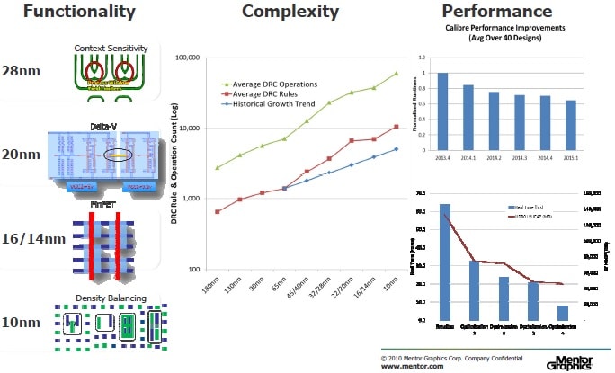
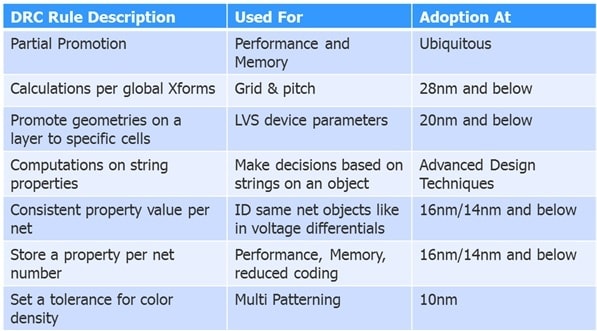
Some examples of these new functionalities are summarized in the following table:
For some of the more complex checks we have been adding automated pattern matching capabilities to DRC design kits which results in a quicker way to define a requirement. It replaces text-based DRC with a visual geometry that ensures precise and accurate implementation of the design specification – a kind of high tech version of “a picture is worth a thousand words”.
We also worked extensively with TSMC for multi-patterning at 10nm because it is critical to get both correct coloring definition and density balancing between different layers. Moreover, we also invested time in the display of any errors caused by this interplay to the designer so they are actionable.
For 3D, Calibre 3DSTACK verifies complete stacked die assemblies. It performs all DRC/LVS and extraction checking for each die and also on the interface geometries between chip designs, including bumps, balls, TSVs, etc., and it supports dies from multiple processes. Key to this product is the use of the sign-off Calibre design kits provided by the foundry that will manufacture the stacked solution.
Q: Let’s look at the role of India in the semiconductor ecosystem. It is true, India has great education system and large presence in semiconductor IP and design creation; most of the design MNCs have their subsidiaries in India. However, in the context of semiconductor foundry and investments, I do not see much push in India; China is doing much better on that. From an overall ecosystem perspective, in my view, these are some key missing elements, and hence India may not see growth according to the potential of its pool of talented workforce. How do you see this? What should be the best alternative for India?
A: Michael: From Calibre perspective, I am super bullish on India. Our Applications Engineering group in India is able to lead on many fronts including helping with existing EDA tool decisions, new tool recommendations, flow recommendations, interfacing with fabs, use models, and so on.
Ruchir: We have been significantly growing the Calibre technical team in India as we see not only growth in the India EDA market but also the influence the India teams have on EDA tool selection decisions at multinational companies.
Michael: I have seen multiple articles about India wanting to have semiconductor fabs in India. But Calibre’s interactions with India design teams, like our engagements in the rest of the world are independent of where the target fab is physically situated. Semiconductors are a global ecosystem and we engage with customers with that perspective in mind.
Ruchir: I agree. Mentor India is actively involved in projects with multiple Indian companies where the designs are targeted to processes and fabs located throughout the world.
Michael: Now to the question of having a foundry in India, naturally cost should definitely be in consideration. Today, many opportunities in IoT, Automotive, and other segments are driving capacity at established nodes. So, a foundry that is focused on supporting established node demand could be good for India.
Q: Mentor Graphics has a very good presence in India with its R&D as well as sales centers, and it is performing a key role in the semiconductor design industry with a wide portfolio of EDA tools. Since Mentor’s Calibre is a key interface to foundries and it is central to the overall semiconductor ecosystem, do you see Calibre influencing the Indian semiconductor community is any specific way?
A: As I said earlier, the role is independent of where the foundries are. Currently we see India’s role in the semiconductor ecosystem, besides the significant multi-national presence in IP in chip design services. We see India as having a very large semiconductor design talent pool with more candidates graduating into the pool each year. So, it makes sense for us to provide localized design and interface services to our customers and ecosystem stake holders there as part of our 24/7 service to the global ecosystem.
Not only has Ruchir increased size of the local Mentor Calibre India team, we have specifically assigned Calibre TMEs (Technical Marketing Engineers) from the Calibre Business Unit to provide additional India support. These Calibre TMEs drive both product and joint efforts with our Foundry Partners providing a next level of expertise to our engagements.
Q: What is the future vision for Calibre in the semiconductor ecosystem?
A: It’s definitely to continue to grow applications in the interface between foundry and design. For example, we are already using extraction techniques developed for FinFETs in the design of MEMs, resulting in extraction design kit development time being reduced from weeks to hours in addition to providing more accurate extraction analysis. We are also doing work in the emerging silicon photonics space to bring software and verification techniques to a design process that historically has been all hand crafted.
This was a very interesting and learning experience for me talking with Michael and Ruchir. Calibre definitely is a key part of the semiconductor ecosystem and it continues to grow its leadership by innovating newer ways to solve increasing challenges posed by newer technologies and designs.
Pawan Kumar Fangaria
Founder & President at www.fangarias.com


Comments
There are no comments yet.
You must register or log in to view/post comments.