

At the recent TSMC OIP symposium, a collaborative presentation by Synopsys and Xilinx highlighted the importance of incorporating the local FinFET device self-heating temperature increase on the acceleration of device reliability mechanisms.
Synopsys has developed a flow for integrating self-heating calculations into the reliability analysis features of their circuit simulation products – e.g., HSpice, CustomSim, FineSim. This enhanced flow is (or soon will be) a required step in tapeout signoff by your reliability engineering team.
Device Aging Mechanisms — Background
There are 3 principal device aging effects that lead to changes in device operating characteristics, for both planar and FinFET devices:
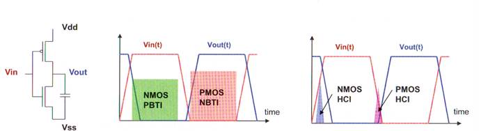
(1) Bias Temperature Instability (NBTI, PBTI)
For the period of device operation when there is a strong electric field between gate and inverted channel, there will be a force on free carriers directed toward the gate dielectric. A density of “trapping states” at the dielectric-channel interface will become filled over time by channel carriers.
There is ongoing research into the origin of these interface trapping states, as a function of the dielectric materials and device operation, including models for both permanent and “recoverable” carrier occupation.
For p-channel devices, the gate-to-channel E-field is negative – this mechanism is denoted as Negative Bias Temperature Instability (NBTI). For n-channel devices, the E-field is positive, and the mechanism is known as Positive Bias Temperature Instability (PBTI).
The net result is an increase in the magnitude of the device threshold voltage |Vt|, and a degradation of the channel carrier mobility. These (probabilistic) mechanisms are reflected in the device aging model.
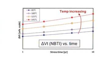
As is implied by the “T” in the name, the |Vt| parameter shift is temperature dependent, due in large part to the temperature dependence of interface trap generation.
(2) “Hot” Carrier Injection (HCI)
The aging mechanism associated with hot carrier injection is similar to BTI – i.e., a shift in device parameters due to the field-directed velocity of channel free carriers toward the channel-dielectric interface.
The HCI difference is that this effect occurs during saturated channel operation, where the carrier energy is very high (and the probability of additional “impact ionization” is increased) in the vicinity of the pinchoff channel depletion region at the device drain node. HCI is more of a drain-localized mechanism, and is primarily a carrier mobility degradation (and a Vt degradation if the device is operated bi-directionally).
With advanced process engineering of the impurity profiles at the device drain node, HCI has become less of a reliability concern – BTI is a much more prevalent mechanism in current processes.
(3) Time-Dependent Dielectric Breakdown (TDDB)
The application of a (low) electric field across the gate dielectric results in “wearout”, and eventually breakdown. This is a (probabilistic) mechanism intrinsic to the dielectric – especially, the density of “weak” chemical bonds – and is therefore represented statistically as a failure rate estimate.
Although TDDB analysis is a key factor for reliability engineering, the intent of device aging models (and their simulation) is to ensure failure-free operation over the product’s lifetime. These models are focused on device parameter shifts due to BTI and HCI.
MOSRA models
The Synopsys team has supported a Reliability Analysis extension to circuit simulation models for several (planar) process nodes, to evaluate the long-term impact of BTI and HCI.
For the greatest flexibility, support is provided for both “built-in” MOSRA aging models, as well as an API to enable a foundry such as TSMC to provide a custom aging model definition (the MOSRA.so library).
The figure below illustrates the waveform-dependent nature of these mechanisms – as described earlier, BTI and HCI depend upon the region of active device operation. The slew rate of the circuit inputs and output will have a significant impact upon these mechanisms, especially HCI.
Unlike planar (non-SOI) devices, FinFET’s have a much higher thermal resistance to the substrate. As a result, there is a self-heating characteristic to the device channel. The channel temperature increase will accelerate BTI/HCI effects over the product lifetime, as illustrated in the figure below from the Synopsys/Xilinx presentation.
(Please note again that the device active power and self-heating delta_T is a strong function of the circuit’s input slew and capacitive loading.)
It is therefore necessary to establish a device aging analysis flow that incorporates the channel delta_T due to self-heating.
The Synopsys Reliability Analysis Device Aging Flow
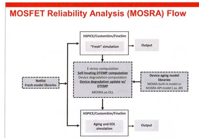
The initial step in the flow is to exercise a “fresh” simulation to derive the pertinent waveforms, and evaluate the interval within the simulation when these effects are active.
Although perhaps obvious, selecting a representative testbench for the fresh simulation is crucial. The aging models will extrapolate these simulation results using an integral equation over the product lifetime of T years (with a fractional exponent for time in the integral, as indicated by the log-linear NBTI plot above).
Also probably obvious, specific focus for fresh simulations should be placed on analog (DC-biased) circuits requiring device matching, and any time period-sensitive macros, such as PLL’s/DLL’s.
The fresh simulation testcase requires an iterative update, to incorporate the effects of each device’s self-heating delta_T (DTEMP) calculation, provided by a separate R_thermal model analysis using the MOSRA API and support from the foundry. The R_thermal model for FinFET layouts is especially sensitive to the device topology – e.g., the values of NFIN and NFINGER for each device.
The converged fresh simulation with self-heating can then be applied to generate predictive aging models for device lifetime interval(s). The results are then compared to the fresh simulation to assess the degradation in circuit performance.
Synopsys has qualified a reliability analysis flow incorporating a device aging model for BTI and HCI with FinFET-based self-heating DTEMP calculations. The recent data presented by Synopsys and Xilinx for a TSMC N16FF design indicates that this flow must become an integral part of your circuit analysis and reliability signoff tapeout criteria.
-chipguy
Share this post via:


Comments
There are no comments yet.
You must register or log in to view/post comments.